Would the fudge factor rather be a statistically significance correction factor for manufacturing tolerances . Not a view that the process is not well understood . Then again fudge factor is a poor and misleading term for what is a range of how well the product is made not how well the physic is understood to make it.Agreed. It sets up the belief that semiconductor physics is not well understood by those who do it for a living.
jn
Would the fudge factor rather be a statistically significance correction factor for manufacturing tolerances . Not a view that the process is not well understood . Then again fudge factor is a poor and misleading term for what is a range of how well the product is made not how well the physic is understood to make it.
When I was working diodes for a living, we had to test diode vf to the 1 millivolt level for binning. We would take diodes from one bin, and parallel 3 of them for the 3 phase 25 amp military bridge legs. For some big diodes, we'd parallel around 50 diodes from 1 bin on nickel plated aluminum rails 1/2 inch by 1/2 inch by 6 inches.
In all cases, the diodes were kept together by diffusion runs. That would give the best current sharing at all currents.
If different diffusion batches were mixed, the diodes in an assembly would still have the exact same vf at the test current, but could have different temperature coefficients as well as slightly different Vf curves. So a unit would meet room temp vf specification which guaranteed current sharing, but if the device were at a different temperature, sharing would be compromised and the unit could runaway. If the test current deviated from the binning current, the resultant vf curve would also deviate. For example, one diode tested at 13 amps, with the paralleled 3 at 39 amps would produce identical vf's, but at currents other than 39 amps for the 3, the vf will not match any device if they are different diffusions.
Taking any diode out of the box so to speak, you cannot guarantee that the vf curve will be exactly the same as the next one out of the box, nor can you guarantee that the temperature coefficients are the same.
Diodes can be made using different diffusion profiles, different wafer (silicon) resistivity, different thickness, epitaxial, different speed enhancing impurities (gold vs platinum), schottky... For the user (you and me), we do not have access to the exact numbers we would need to characterize the full Vf vs I vs Temp, so we either test for the curves of the device, or we try to fudge it by making the circuit stable for some small range of device parametric.
The equations can be quite exacting...but those of us out in the field can't get the numbers we would require.
I would tend to believe that an astrophysicist generally doesn't have the experience gained from working a semiconductor diode production line from wafer to potted product to be able to detail such issues with real diodes, so cannot go past "fudge factors" as an explanation. Nonetheless, such verbage doesn't address much, it's kinda like "pay no attention to the man behind that curtain"
jn
Last edited:
Would the fudge factor rather be a statistically significance correction factor for manufacturing tolerances . Not a view that the process is not well understood . Then again fudge factor is a poor and misleading term for what is a range of how well the product is made not how well the physic is understood to make it.
For decades already in between the wafer saw lanes most IDE's have had a set of standard ref components that are measured and the data is fed into models to keep the process on track, but also as part of the characterization process.
Most good processes run at yields in the high nineties nowadays. You don't get that kind of performance without an intimate knowledge of the device physics and the process chemistry. There may be a FEW very esoteric processes (like GHz Power devices for example) where there are process adjustment factors, but there are no 'fudge factors' that I am aware of.
Last edited:
Thus for you the correction factor is very small due to tighter controls. Jneuton points out much what I have experienced in the field there are greater variances than in the lab. I do like the man behind the curtain analogy . Off to see the wizard now . RegardsFor decades already in between the wafer saw lanes most IDE's have had a set of standard ref components that are measured and the data is fed into models to keep the process on track, but also as part of the characterization process.
Most good processes run at yields in the high nineties nowadays. You don't get that kind of performance without an intimate knowledge of the device physics and the process chemistry. There may be a FEW very esoteric processes (like GHz Power devices for example) where there are process adjustment factors, but there are no 'fudge factors' that I am aware of.
I don't know is it for AB. It's from Scotch attachment in other thread. I think !
That's just a diamond variant no correction per se.
Regarding the OPS of anything -- including IC amps ---- anyone done work on furthing the reduction of switching distortion in AB amps? This is an interesting way which I wonder has it been used/refined somewhere..... Oct 1980 AES preprint 1683 (D-4) by G.Dodson of JBL. "Quasi-Class A/Improved Class AB Bias Loop"
View attachment 455325
THx-RNMarsh
dynamic bias appears to be very good.
View attachment Bias.pdf upside down!
Happy Holidaz, to all the gang members at DIY !
")
THx-RNMarsh
Last edited:
Almost any modern class AB scheme will appear linear if you are looking directly at the output at crossover. To see and compare the errors you need to make a Vin-Vout comparison, and you can look at the derivative of that to see the details very well.
Kenpeter liked to use Schottkeys in that circuit, which produce pretty much the same blip as BJTs do, just more gradually due to a different exponential slope. The diodes also don't heat up nearly as dramatically as power transistors do, so theoretically they will have better thermal behavior.
http://www.diyaudio.com/forums/soli...r-non-switching-need-revival.html#post2149538
dynamic bias appears to be very good.
View attachment 455498 upside down!
Happy Holidaz, to all the gang members at DIY !
THx-RNMarsh
Edmond Stuart's "AB2" error correcting non-switcher is simpler than a LT1166.
Yamaha's "hyperbolic" circuit is the discrete equivalent to the LT1166 .
They are both "slow". They "Gobble" up a CFA's slew rate in big bites.
Repaired a yamaha "hyperbolic" - NO noticeable superior performance ...
in fact - A CFA w/ standard EF3 beats it. NO holy grail here - build a Class A.
In simulation (besides being slow) they do reduce H3/5/7 "slightly" ....
Edit - JVC's "super A" IS noticeable - I'd love to reverse engineer thier
dynamic bias circuit.
OS
Last edited:
Purely historically, the idea of a sliding bias commerically appeared around the mid-70ies, as far as I can tell, from JVC.
At the time, their sales blurb stated that their system allows us to listen to a pure class A sound all the way, but minus the penalty of making the amp conduct in classic pure class A all the time, thus producing much less unwanted heat, saving of otherwise wasted energy and allowing for smaller heat sinks. If memory serves, a few of their integrated amps of the day did sound a buit cleaner than most in their price range.
Before you knew it, everybody and their dog had some form of that system. As far as I can determine, the furthest anyone went in that direction was achieved by Marantz, who throughout the 80ies offered their quarter A system, which allowed the amp to run in pure class A up to 1/4 of its nominal power. Others, like Yamaha, eschewed such an approach and offered a switch, which when flicked reduced the overall power supply line voltages, but made the amp go into puire class A on a lower power level.
Initially, the High End of the day all but ignored this, until Krell produced amps with a switch for "normal" and "high" bias. Then they evolved this simple approach to what they call "Sustained Plateau Bias", which initially used a very high speed op amp to anticipate the incoming signal and open up the bias circuits to accept it, the theory being that this opening up would happen before the signal reached the output stage, which would thus be ready to pass it on in class A mode.
The advent of ever more and ever cheaper digital ICs appears to have prompted then to evolve this approach into an entire system; these days, you need to take a vacation to backtrack what they do, their late 90ies models use 118 transistors per side just for the input stage and the VAS.
The idea, it seems to me, is good enough to merit some word using current day technology, unavailable at the time of thsi approach inception.
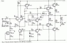
Here is the original.
I recall you had a single diode version before this one in an amp you sold. One day, a new technician employee at LLNL who had worked for you had a copy of your schematic which he showed me... a single diode from output to bias circuit to bump up the bias with signal level. Can you show that also now?
In this time of the Blameless amplifier.... the OPS is the weak link. We have the EF and the complimentary pair for OP device. What more can be done to make the OPS better under load and current demands? Besides Class A. I have seen some good work here but more needs to be done. IMO.
THx-RNMarsh
Last edited:
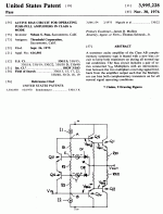
I think you are referring to the 1978 Audio Amateur "A40" which was simply
an auto-bias circuit. Note that the output devices are Darlingtons with
two diode drops.
Yes, that is what I was shown by tech. He had full size sheet schematic.
Also, TAA. Auto bias.
Looked like maybe a precursor to the patent idea you show.The post ESS amplifier era in Sacramento.
THx-RNMarsh
Last edited:


 merry CHRISTmass to you all
 Looked like maybe a precursor to the patent idea you show. The post ESS amplifier era in Sacramento.
This was '78. The sliding bias stuff came from '74, but this was a lot simpler
for beginning DIYers.
It will amuse you that Barry Thornton (one of the non-switching patents)
was in Sacramento also, and was loosely associated with ESS before I
arrived there in '72. I met John Curl in '73.
memory lane --
I know him well.... before ESS he ran an audio store where we met near El Camino ave (next to Tognotti's). Later he moved but kept a house (near Placerville) and asked if I wanted to rent it.... he wasnt sure how long his new job (Arizona I think) would last. But he never came back and I lost track of him. he loved electronics but for some reason... at the time I knew him he didnt have an electronics degree, he told me. He had a BA in some off the wall subject. Quite inventive and creative guy. Last time I saw him was when ESS was bankrupt and I was asked to help go thru inventory with a friend (Dave Cusker?) of the foreign investor. I have no idea anymore what I was doing at the time.... probably still in Livermore at LLNL. People just seem to find me somehow as I try to keep a low profile. Later, you opened your shop up the hill from where I now reside.... and the rest is history with your Pass Labs equipment. Where is B.T. now?
THx-RNMarsh
This was '78. The sliding bias stuff came from '74, but this was a lot simpler
for beginning DIYers.
It will amuse you that Barry Thornton (one of the non-switching patents)
was in Sacramento also, and was loosely associated with ESS before I
arrived there in '72. I met John Curl in '73.
I know him well.... before ESS he ran an audio store where we met near El Camino ave (next to Tognotti's). Later he moved but kept a house (near Placerville) and asked if I wanted to rent it.... he wasnt sure how long his new job (Arizona I think) would last. But he never came back and I lost track of him. he loved electronics but for some reason... at the time I knew him he didnt have an electronics degree, he told me. He had a BA in some off the wall subject. Quite inventive and creative guy. Last time I saw him was when ESS was bankrupt and I was asked to help go thru inventory with a friend (Dave Cusker?) of the foreign investor. I have no idea anymore what I was doing at the time.... probably still in Livermore at LLNL. People just seem to find me somehow as I try to keep a low profile. Later, you opened your shop up the hill from where I now reside.... and the rest is history with your Pass Labs equipment. Where is B.T. now?
THx-RNMarsh
Last edited:
- Status
- Not open for further replies.
- Home
- Member Areas
- The Lounge
- John Curl's Blowtorch preamplifier part II