Ah, thank you, it was me indeed! It's the bad way I expressed myself again. What I really meant was that I didn't see one with output impedance that is flat across, with no peaks above 1 milliohm, all the way to 10MHz.
Here's a plot I used a while ago when comparing to some popular regulator: lhs plot is the popular regulator, rhs plot shows what I was trying to say and failed. Obviously, we're in the fairy land of simulators here.
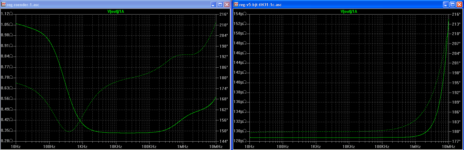
Here's a plot I used a while ago when comparing to some popular regulator: lhs plot is the popular regulator, rhs plot shows what I was trying to say and failed. Obviously, we're in the fairy land of simulators here.
As you see, the output impedance peaks at 5milliOhm at around 1MHz
Is this a simulation of the circuit on the left, or the circuit with parasitics (output cap L, ESR, etc)?
Is this a simulation of the circuit on the left, or the circuit with parasitics (output cap L, ESR, etc)?
Yes, no parasitics considered. Simulation I was asked, simulation I provided. As I said, I have no means to directly measure the output impedance. My estimate is around 10milliohm (in the MHz range), with SMD parts and force/sense wiring.
BTW, your estimate of parasitic reactances you posted a few pages up was 3 orders of magnitude off.
BTW, your estimate of parasitic reactances you posted a few pages up was 3 orders of magnitude off.
I know, I'm in a hurry and I edited my post:
Yes, syn08, I omit 10^-3
Ah, thank you, it was me indeed! It's the bad way I expressed myself again. What I really meant was that I didn't see one with output impedance that is flat across, with no peaks above 1 milliohm, all the way to 10MHz.
That's an easy one. Just play with the gate resistor and, while you cannot cancel the peak (a pole is a pole, and is certainly a pole
") ), you can easily bring it under 1milliohm. Depending on the MOSFET type, try around 300ohm.
), you can easily bring it under 1milliohm. Depending on the MOSFET type, try around 300ohm.So hang on there Steve. Your mind is alive and you think clearly.
There are some here that disagree with that.
Well, everyone, I am from the 'old school' of designers, as you well know.
This reminds me of a situation that I had at Cal Berkeley, while waiting for an engineering class to begin. I was in the 'canteen' having a cup of coffee, when some fellow students who attended my class were discussing an engineering problem at the next table. Our professor had previously assigned some homework vaguely similar to what Syn08 is appearing to be telling me that I am missing out on. It was mathematically elegant, sophisticated, yet the student worrying over the problem could not figure out what a factor of 10 was in the middle of the set of equations.
I glanced over and pointed out that the factor of 10 was Gm Rl or the voltage gain of the fet stage that we were analyzing. Yes, the point of the exercise had been completely obscured by the math. Such is a university education, sometimes. However, I was not merely a student, at the time. I had 5 years experience as a designer in an engineering firm, under my belt, before I took this course. I learned my design rules from other engineers, on the office.
I could see the problem from inspection, and a slide rule. It is the same here. Gm Rl = the gain of the noise More Rl, more noise. More Gm, more
noise. Super high Idss gets you medium Gm, VERY LOW R = less noise
However, low Gm, and medium Idss allows LOW R and LOW Gm times LOW R gives a good result also. It must be remembered that Gm FOR A GIVEN DEVICE GEOMETRY changes as the square root of the Idss, but the Rl DROPS in value directly with Idss. Therefore, there is an advantage in using higher Idss WITH THE SAME DEVICE GEOMETRY, in this design example.
Last edited:
Well, everyone, I am from the 'old school' of designers, as you well know.
This reminds me of a situation that I had at Cal Berkeley, while waiting for an engineering class to begin. I was in the 'canteen' having a cup of coffee, when some fellow students who attended my class were discussing an engineering problem at the next table. Our professor had previously assigned some homework vaguely similar to what Syn08 is appearing to be telling me that I am missing out on. It was mathematically elegant, sophisticated, yet the student worrying over the problem could not figure out what a factor of 10 was in the middle of the set of equations.
I glanced over and pointed out that the factor of 10 was Gm Rl or the voltage gain of the fet stage that we were analyzing. Yes, the point of the exercise had been completely obscured by the math. Such is a university education, sometimes. However, I was not merely a student, at the time. I had 5 years experience as a designer in an engineering firm, under my belt, before I took this course. I learned my design rules from other engineers, on the office.
I could see the problem from inspection, and a slide rule. It is the same here. Gm Rl = the gain of the noise More Rl, more noise. More Gm, more
noise. Super high Idss gets you medium Gm, VERY LOW R = less noise
However, low Gm, and medium Idss allows LOW R and LOW Gm times LOW R gives a good result also. It must be remembered that Gm FOR A GIVEN DEVICE GEOMETRY changes as the square root of the Idss, but the Rl DROPS in value directly with Idss. Therefore, there is an advantage in using higher Idss WITH THE SAME DEVICE GEOMETRY, in this design example.
I couldn't put it in a more complicated/confusing language, but slowly, slowly is going there
It must be again pointed out that some jfet geometries, have more Gm@Id than others. The reason for this is related to the geometry, for example LONG GATE devices tend to have lower Gm@Id, while SHORT GATE devices have higher Gm@Id.
Also, all jfet geometries have higher Gm:Id ratio when operating at lower currents, in this case Idss. Therefore, a higher Idss part has a lower Gm:Id ratio and this justifies a smaller Rl as well, so the total noise gain is less than a lower Idss part.
So for a GIVEN Idss, the long gates will tend to perform better as a current source, since they won't amplify their own noise as much, and higher Idss long gate devices will be quieter in this case, as well.
Now comes the hard part, what is the intrinsic noise of the jfet under consideration? This is where data books, Quantech Noise Analyzers, or their equivalent, experience, and a little Van der Ziel comes in handy.
It so happens that the base noise of a jfet is approximately: R(noise) = 2/3 times 1/Gm. For example: the base noise of a 4000 mS fet at 6ma,(2SK246) might be 250 times 2/3 = 170 ohms or about 1.7 nV/rt Hz. You won't get better than this with this Gm in a fet at room temperature and above.
Now look at a 2SK170: Gm at 6ma is: 33,000 mS, 20 ohms noise eq. Big difference! and the noise could possibly be as low as 0.58nV/rt Hz Pretty darn good, about 1/3 the noise of the 2SK246. However, with the SAME Rl, the 2SK170 will measure worse, just like Syn08 measured. This is because the Gm of the K170 is 8.2 times greater than the K246. Noise times Gm times Rl =?
Please, those who can, do the math, yourself.
Also, please understand that LOW NOISE JFETS are not just any fet. They are processed for minimum 1/f noise at audio frequencies. Many jfets will not work very well because they were made more cheaply, perhaps as a switch, and can have a lot of excess noise.
Last edited:
Well, is everybody ready for the quiz in Friday? ;-)
In retrospect, it is easier to understand what I am getting at, IF you look closely at the data sheets of the jfets involved.
I might also say that there are other possible reasons why the PN4392 seemed to do better than expected, even with low Rl. This is because of higher operating temperature that lowers the Gm from its nominal value, and its relatively high output conductance with only 5V or so across the device. These would be minor matters, but I estimate that the Gm at 47 ma would be about 25,000 mS at most. This is kind of low. Just put eight six ma Idss 2SK170's in parallel to match 48 ma, and what do you get? 8 X 33,000 ms or about 250,000 mS or about 10 times more noise gain. See the problem?
And how hot did Syn08 run his PN4392? I would not want to put my finger on it. This is because the device he selected is designed to run in a heatsink. Without a heatsink, very hot internal temperatures, indeed. This can be seen from the spec sheet for the device in the 'NT Transistor Databook 1982 ' p.3-2 It is a T0-18 metal can with limited dissipation. He is operating at 250mW or so. Unless Syn08 is using a special T0-18 heatsink, (they make them) or a Freon bath, he is running hot. This will lower the Gm, and therefore, the noise gain of the device.
Last edited:
Well, is everybody ready for the quiz in Friday? ;-)
In retrospect, it is easier to understand what I am getting at, IF you look closely at the data sheets of the jfets involved.
I might also say that there are other possible reasons why the PN4392 seemed to do better than expected, even with low Rl. This is because of higher operating temperature that lowers the Gm from its nominal value, and its relatively high output conductance with only 5V or so across the device. These would be minor matters, but I estimate that the Gm at 47 ma would be about 25,000 mS at most. This is kind of low. Just put eight six ma Idss 2SK170's in parallel to match 48 ma, and what do you get? 8 X 33,000 ms or about 250,000 mS or about 10 times more noise gain. See the problem?
And how hot did Syn08 run his PN4392? I would not want to put my finger on it. This is because the device he selected is designed to run in a heatsink. Without a heatsink, very hot internal temperatures, indeed. This can be seen from the spec sheet for the device in the 'NT Transistor Databook 1982 ' p.3-2 It is a T0-18 metal can with limited dissipation. He is operating at 250mW or so. Unless Syn08 is using a special T0-18 heatsink, (they make them) or a Freon bath, he is running hot. This will lower the Gm, and therefore, the noise gain of the device.
Indeed, the PN4392 was running pretty hot, dissipating some 250mW. However, the big gap in transconductance (I see you still insist in using Gm, although it's quite confusing here, as I said, for a fixed output voltage Vo, the noise gain does NOT depend directly on the transconductance) is not because the temperature, but because of the high pinch voltage Vt. A typical K170 has say Vt=0.2V while the PN4392 has about Vt=4V. Hence, a x20 factor in transconductance (or x20 in 2*Vo/Vt, the gain noise).
BTW, check your numbers. 25,000 milliSiemens = 25 Siemens 33,000 milliSiemens=33 Siemens. That's a stretch
Perhaps microSiemens?
Last edited:
That's an easy one. Just play with the gate resistor and, while you cannot cancel the peak (a pole is a pole, and is certainly a pole
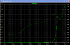
Sorry guys, you're going too fast for me. This is how it simulates for me, the exact circuit you showed, except I'm using lm129 for reference, and all capacitors have parasitics 0R5 ESR and 5nH ESL.
Increasing the gate resistor does not reduce the bump.
I'm using ltspice (too much of a pain to load orcad now), but that should not be a problem. The simulator is set for maximum accuracy (v small tolerance and step size, no compression, etc.).
I'd also like to point out, regardless of these plots, that just because one uses the absolute lowest noise reference in a circuit, it does not mean that the noise a the output of the circuit is very low.
It's unfortunate that I can't simulate John's circuits; it's a bit unfair to syn08, even though he doesn't actually use this particular regulator.
Anyway, please don't shoot, I'm just a beginner trying to understand what you guys are doing and learn from your experience.
Attachments
I'm just a beginner trying to understand what you guys are doing and learn from your experience.
Learning pretty fast, indeed.
This is how it simulates for me, the exact circuit you showed, except I'm using lm129 for reference, and all capacitors have parasitics 0R5 ESR and 5nH ESL.
Not sure if you are aware of, but that's precisely why I avoid like plague any discussions about simulations. Unless people do calibrate models and simulating conditions, such discussions are going nowhere. Said by a bloke who in another life used to work for Cadence Systems.
Anyway, 0.5ohm and 5nH parasitics are between one and two orders of magnitude larger than those for 0805 SMD parts. FIY, 5nH is the inductance about 1cm of bare, straight wire in free space.
Well, is everybody ready for the quiz in Friday? ;-)
My dog ate my #2 pencil.
se
I'm so old that I confuse umhos with mS. That is the problem.
Never mind, you are doing pretty well for your age
Not sure if you are aware of, but that's precisely why I avoid like plague any discussions about simulations. Unless people do calibrate models and simulating conditions, such discussions are going nowhere. Said by a bloke who in another life used to work for Cadence Systems.
Anyway, 0.5ohm and 5nH parasitics are between one and two orders of magnitude larger than those for 0805 SMD parts. FIY, 5nH is the inductance about 1cm of bare, straight wire in free space.
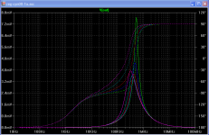
I removed all parasitics. It looks more like your initial plot. I stepped the gated resistor as follows 50R 150R 300R 600R 1200R
Please read the Y axis as ohms, I forgot to divide by 1A.
The bump goes down for a bit, but then it goes up. I would have been really surprised if it was so easy to get rid of that pole, even for experts. It took me weeks to solve this problem. Not that it matters, it's just a simulation anyway, it gets thrown out the window as soon as the solder hits the pad.
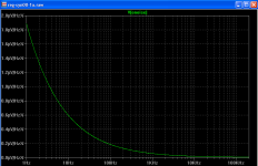
For what it's worth, my earlier Zout example was simulated with full exaggerated parasitic ESR and ESL.
On a different topic, my calculations don't exactly agree with yours as far as the noise of the Norton equivalent goes. I have to double check though.
Sorry, I hate being a pain (and so slow), but I think it's in everyone's best interest that we do this carefully.
Attachments
- Status
- Not open for further replies.
- Home
- Member Areas
- The Lounge
- John Curl's Blowtorch preamplifier part II