Also I was reading the original Article which used the supply to opamp taken before the pass Transistor with filter caps.Did you change that in new boards to avoid oscillation?
Oscillation??
Feeding the opamp from the regulated voltage rather than the raw voltage with junk improves the result.
The only issue is start-up - conceivably, powering the opamp from its own result might not start it up - chicken and egg. Fortunately, it does.
Jan
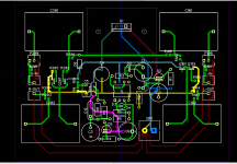
The logic seems OK but I think it can be much more compact. How many layers is this, what is the layer assignment?
I would move the supply connector between C2 & D2, short run to the C of Q1, and much shorter supply ground lines. But depends a bit on your layers.
You can use through holes to swich a track from top to bottom.
Edit: some part dwesignations are inside the footprint, meaning you don't see them anymore after assembly. A bitch when fault searching. Better to move the designations so they remain visible.
Jan
Last edited:
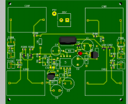
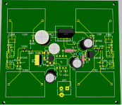
ok, I removed the big heatsink,as the current draw is less than 40mA. The input will be only 24V. So close to a 1/4 watt dissipation. a small heat sink would be enough?
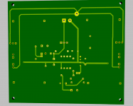
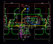
The board is two layer,ground traces and raw power are on bottom and top for analog signals.
Using different color traces to identify
Yellow is power ground
Blue Raw DC
The board is two layer,ground traces and raw power are on bottom and top for analog signals.
Using different color traces to identify
Yellow is power ground
Blue Raw DC
Attachments
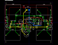
Getting better, although you could have kept the heatsink, there's lots of space up there.
Anyway. One more step would be to clean up the tracking to the big caps, these are much too long, take the direct routes as much as poossible, limit loop area.
Also, the brown? red? - same thing.
For an example, see attached, red ground trace example.
Jan
Anyway. One more step would be to clean up the tracking to the big caps, these are much too long, take the direct routes as much as poossible, limit loop area.
Also, the brown? red? - same thing.
For an example, see attached, red ground trace example.
Jan
Attachments
Last edited:
I am still using a heat sink but changed to less bulky type as the calculated power dissipation is less than 0.5 W even if I use a 30V raw DC supply.
This is the new heat sink
274-3AB Wakefield-Vette | Mouser
Jan, thanks for suggestion.
How important is it to keep the resistor capacitor at positive sense line R16,C12( in my board R8 , C12) ? Is it only useful when long cables are used?
And what type of ceramic cap is recommended? Like an Smd x7r?
Last edited:
These little heatsink are usually rated around 20C/W, 9C/W is unusually low.
0.5W into 9C/W raises the sink to 4.5Cdegrees above ambient before applying the de-rating factor. Try guessing a DF =2 gives a deltaT ~ 9C = very cool.
Even using a 20C/W would probably give a deltaT ~ 15C to 20C, still pretty cool or just warm.
0.5W into 9C/W raises the sink to 4.5Cdegrees above ambient before applying the de-rating factor. Try guessing a DF =2 gives a deltaT ~ 9C = very cool.
Even using a 20C/W would probably give a deltaT ~ 15C to 20C, still pretty cool or just warm.
How important is it to keep the resistor capacitor at positive sense line R16,C12( in my board R8 , C12) ? Is it only useful when long cables are used?
And what type of ceramic cap is recommended? Like an Smd x7r?
Not used unless you use remote sensing.
Jan
Reducing traces further might need some real talent. I used smd cap and resistor for the filter (R8 C12),still not sure it is needed.
heatsink is smaller.
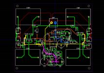
If you look at the 2nd and 3rd pic, the traces to the big caps make huge detours! Make them as direct as possible, to limit length and loop area.
Also, your traces are unusually fat which limits your tracking options also.
(I'm not saying it won't work, but since we have this exchange, why not go all the way ;-).
Jan
Attachments
Last edited:
OK, I will just continue until you get fed-up ;-)
Look at the huge open space around that poor R206, also R106, 102. That can be much more compact. It would also unleash a whole slew of shoving parts around, making the PCB maybe 20 or 30% smaller, and you may not want to do that.
What is the PS1 pin; what are the brown (hardly visible) tracks doing there all the way out?
Jan
Jan, I won't get fed up ") . A better design is every DIYers dream.
. A better design is every DIYers dream.
I want to leave some space around Jfets(10x10 mm) to stick a heat sink to couple them thermally. They are going to run hot perhaps near their maximum power dissipation near 300mW.
I want the board to be little more compact length wise and work on it today, now it is about 10cmx 8.8 cm. I do not want to make it much smaller as I want to stuff boutique caps on board if it work out great .
PS1 is the star point where analog and power supply ground meet. I left a temperory pad there but once board is finalized ps1 will go. Those brown traces( actually red,but being on under surface giving them brown tint) are seperate grounds from input and out put.
I left the power supply ground trace twice thicker(1.2mm) in pcb.
Please let me know your thoughts.
. A better design is every DIYers dream.I want to leave some space around Jfets(10x10 mm) to stick a heat sink to couple them thermally. They are going to run hot perhaps near their maximum power dissipation near 300mW.
I want the board to be little more compact length wise and work on it today, now it is about 10cmx 8.8 cm. I do not want to make it much smaller as I want to stuff boutique caps on board if it work out great .
PS1 is the star point where analog and power supply ground meet. I left a temperory pad there but once board is finalized ps1 will go. Those brown traces( actually red,but being on under surface giving them brown tint) are seperate grounds from input and out put.
I left the power supply ground trace twice thicker(1.2mm) in pcb.
Please let me know your thoughts.
One thing you could do is move those big caps inward, so that the mounting holes can be next to them on the outside. That makes the PCB smaller.
On the brown traces: I know what they are but why are they so far out. They could run underneath the big caps and halve track length. Also with this small PCB you can use a single track on each channel from in- and out ground to the central point.
Jan
On the brown traces: I know what they are but why are they so far out. They could run underneath the big caps and halve track length. Also with this small PCB you can use a single track on each channel from in- and out ground to the central point.
Jan
Attachments
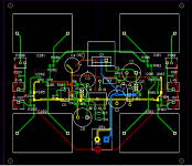
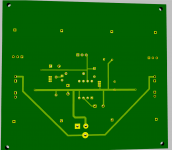
Look at the PSU ground track in the 3rd fig... ;-)
Jan
Jan,Sorry could not figure out what I did wrong there?
Jan,Sorry could not figure out what I did wrong there?
The square angles? Electrons will have to slow down to take those 90 degree turns. ;-)
Jan
Well, the electron drift velocity in copper is in the order of 20 µm/s...Electrons will have to slow down to take those 90 degree turns. ;-)
Quite a lot amount of time to take a 90 degree turn - don't you thing so, too?
Electric field, Poynting vector and the like might be other story.
Ulli ,-)
- Home
- The diyAudio Store
- Super Regulator