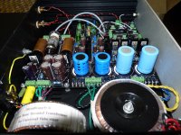
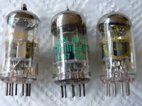
[FONT=Tahoma, sans-serif]Professionaly built 1865 DAC. As good as no use. Built in 2011 by a techical engineer. At the moment Siemens 6922 in the outputstage. Will deliver with other tubes. Looking for € 650.[/FONT]
[FONT=Tahoma, sans-serif]The tube output board is a UTS board designed by [/FONT][FONT=Tahoma, sans-serif]Thorsten Loesch[/FONT][FONT=Tahoma, sans-serif], the designer of the [/FONT][FONT=Tahoma, sans-serif]AMR CD-77 TDA1541[/FONT][FONT=Tahoma, sans-serif] CD player. A 200R resistor is used for I/V conversion. The 0.2V (peak) is then amplified 15x by the ECC88 tube to give just over 2V RMS output from the RCA jacks for a full scale digital signal. The ECC88 is loaded with a constant current source (CCS), the 10M45, and instead of the output being taken directly from the tube plate (anode), it is taken from the cathode of the IXYS 10M45. Regardless of the voltage that is being amplified, the current through the tube remains constant, resulting in the best linearity and least distortion, the bonus being that the output impedance is much reduced over taking the output from the plate of the tube. In this case,output impedance is 300R. Downside of using a mu output is that PSRR(rejection of noise from the power supply) is greatly reduced, so the HT power supply needs to be very quiet and clean. Which it is. It is regulated. Also, the 6.3V for the tube heaters is also regulated. The output is coupled to the RCA jacks with an Obbligato film cap.[/FONT]
[FONT=Tahoma, sans-serif]The digital section of the board is pretty much an exact duplicate of the classic AN design. CS8414 receiver, 74HC02 logic gate/invertor, coupled to the AD1865 DAC chip. SPDIF input is coupled via a pulse transformer and buffered. The DAC chip itself is a 'K', the highest grade[/FONT]
[FONT=Tahoma, sans-serif]The analogue section of the board is disabled by cutting the +15V/-15V copper traces that supplied power to the output stage and removing the 2 resistors that supplied the signal from the DAC chip to the original output stage. The 15V regulators that are upstream of the 5V regulators have to work harder. Disable the audio part of the circuit that we are not using and the 15V regs only supply a tiny ammount of current to the 5V regs which in turn, supply to the analogue sections on the AD1865 chip. In a perfect design, we would have completely separate circuits for the analogue sections of the AD1865 chip and the analogue output stage. Because the 5V is now double regulated. First by the 15V reg (which used to power the analogue stage) and then by the 5V reg. The reason that the +15V/-15V circuit traces are cut, rather than just removing the regulators, is that as well as supplying +15V/-15V to the transitor output stage, there are also additional +5V/-5V regulators powered from the 15V regulators which are used for the AD1865 chips analogue sections. [/FONT]