Here’s a unique little amp I’ve designed for my study with 20kHz THD rather under 0.001% at full power, using common “garden variety” transistors. In my study, I only require low power, and I like to have something to warm my feet on in winter, so the amplifier is rated at 12W rms into 4 ohms. Dissipation per channel is about 50W and quiescent current stability is rock solid.
I call the circuit unique because I’ve come up with a complementary VAS stage which allows the twin long tail pair (NPN/PNP) input stage topology to be used, whilst retaining current mirror loading and push-pull drive to each VAS stage. This significantly improves the linearity and gain of the long tail input pairs over typical circuits that use a low value resistors for the collector load for each LTP. I acheived this by using a differential stage for each VAS and picking-off the biasing point from the non-inverting side of the current mirror. This method works quite well, without compromising PSR.
In order to make the complementary VAS stages as linear as possible, I used both emitter follower buffering, emitter-degeneration and cascoding. Also, a triple emitter follower output stage is used, to keep the loading of the VAS very light.
The quiescent current of the VAS stage is inherently temperature compensating (note the extra diode connected transistor in each current mirror), and is set to 10mA with RV1 (to compensate for the Vf variations of typical red leds). I didn’t use a Vbe multiplier to bias the output stage, as they don’t perform very good when the emitter-emitter voltage of the output transistors is large, as it is in typical class A designs. Iq is set to 1.5A by RV2, giving 1V emitter-emitter, with a ballast resistance of 0.333 ohms in each leg. Temperature compensation is provided by the six transistors connected as diodes. Four of these transistors are TO-126 types, which mount easily onto the heatsink. The pre-driver transistors and their respective temperature compensation transistors are TO-92 types, not mounted on the heatsink, but thermally bonded to each other in pairs.
Separate, unregulated supply rails are provided for the output stage and the low-power circuits. The ~ +/-15V rails for the output stage are provided by a conventional PSU using a twin 12V secondary windings and 18800uF per rail (2 by 4*4700uF). The ~ +/-20V rails are provided also provided with a conventional PSU, but with a transformer having twin 15V secondary windings.
I’m currently laying out the final PCB’s. If anyone is interested in the design, I’ll post the final design files here in the future along with photos of the finished product.
Cheers,
Glen
http://users.picknowl.com.au/~glenk/CLASSA.gif
Hi Glen
Have you tried a more simple topology like this one here http://www.diyaudio.com/forums/showthread.php?postid=1120959#post1120959 for symetrical diff input current mirror loading and push-pull drive to each VAS stage?
And if so, how does it compare to your developped circuit?
12W rms is not much. Are you sure your amp can handle dynamic music transient even at "low" level setting ? Do you think that your circuit could be also used in class AB (higher supply but same actual bias current)? This is what I have done for my amp (15 Wrms class A/ 75 Wrms class B).
fab said:Hi Glen
Have you tried a more simple topology like this one here http://www.diyaudio.com/forums/showthread.php?postid=1120959#post1120959 for symetrical diff input current mirror loading and push-pull drive to each VAS stage?
And if so, how does it compare to your developped circuit?
G'day fab.
I haven't seen it done that way before - there is always more than one way to skin a cat
")
My circuit may be more complex, but it doesn't compromise the operation of the current mirror.
12W rms is not much. Are you sure your amp can handle dynamic music transient even at "low" level setting ? Do you think that your circuit could be also used in class AB (higher supply but same actual bias current)? This is what I have done for my amp (15 Wrms class A/ 75 Wrms class B).
I've got an old but good pair of speakers from an old PYE record player in storage. I used to drive these with a pair of National LM380's as a teenager, and they could be heard a few houses down the street.
Coupled to my baby 12W class A amp, they'll be plenty loud enough for my study.
Cheers,
Glen
G.Kleinschmidt said:
I’m currently laying out the final PCB’s. If anyone is interested in the design, I’ll post the final design files here in the future along with photos of the finished product.
Cheers,
Glen
Hi Glen,
I'm interested !! pls keep us informed. I also interested with your PCB layout, there is no way I can make my own layout for such complex design

thanks alot
G33/33
BBZZZZZTTTT.....
The schematic I posted above is flawed. The current current steering ability of the VAS stages won't work reliably. I was mislead by a spice simulation and my physical prototype unit just worked by a fluke of transistor matching.
I have fixed the topology with a rather simple modification though, and am updating the schematic at the moment.
I have deleted the old schematic and I suggest that anyone who has downloaded it should do also, as the circuit won't work as drawn.
Cheers,
Glen
Okay boys and girls.......
The link (as above) is now attached to the updated schematic, with the revised VAS stages. The LTP load's are now two pairs of CCS's and the VAS drive is fully differential. Anyone who saved the previous schematic, please delete it and swap it with this one.
http://users.picknowl.com.au/~glenk/CLASSA.gif
Comments/Criticisms?
Cheers,
Glen
G.Kleinschmidt said:... I didn’t use a Vbe multiplier to bias the output stage, as they don’t perform very good when the emitter-emitter voltage of the output transistors is large, as it is in typical class A designs. .]
Can you explain why Vbe mult is no better than a pot?
fab said:Only C8 and C9 are required for stability? no cap across feedbcak resistor?
Yes they are.
Have you looked at square wave into RC parallel load yet?
When the final boards are finished, that's what I'll be doing to find the optimum value for C8 and C9.
The traditonal "zobel" only consists of C20? no series resistor?
This is one derivation of the circuit that doesn't need a resistor in series with C20.
I am not sure to see the "current mirror" in the LTP...
Thats probably because the circuit has since been modified and each current mirror has been replaced with a pair of current sources - like I said above.
Cheers,
Glen
Re: Re: My new mini Class A amp.
I did not say that a Vbe multiplier is no better than a pot. I said that a Vbe multiplier isn't very good at biasing a class A stage when the quiescent emitter-emitter voltage across the output stage ballast resistors is large. In this design it is 1V, to give a quiescent current of 1.5A. A Vbe multiplier is substandard in this application because it provides overcompensation. If you don’t believe me, get out a pen and paper and do the math.
Also, I am not biasing my output stage only with a trimpot, but with a trimpot in series with six diode-connected transistors.
Cheers,
Glen
fab said:
Can you explain why Vbe mult is no better than a pot?
I did not say that a Vbe multiplier is no better than a pot. I said that a Vbe multiplier isn't very good at biasing a class A stage when the quiescent emitter-emitter voltage across the output stage ballast resistors is large. In this design it is 1V, to give a quiescent current of 1.5A. A Vbe multiplier is substandard in this application because it provides overcompensation. If you don’t believe me, get out a pen and paper and do the math.
Also, I am not biasing my output stage only with a trimpot, but with a trimpot in series with six diode-connected transistors.
Cheers,
Glen
BBBBBZZZZZTTTTTTT #2
Sorry folks - I've deleted the schematic again. It still won't work . Due to the extremely high gain of the current source loaded LTP's, only a very small Ic imballance in one LTP stage can throw one of the VA stages out with respect to the other, to a degree that cannot be corrected by the DC negative feedback. This is a problem with the symetrical VAS topology, as each VA stage forms the current 'reference' for the other. The circuit works fine in spice, where all the components are identical and have 0% tollerance, but building a real working version is another matter......
I can easilly fix this problem by drastically reducing the LTP stage gains with resistive loading, but that completely overrides any benefit of having a pair of current source loaded LTP's.
It looks like I'm going to have to add a pair of DC servo's to steer the VA stages.
Damn it! And it looked like it could be done so simply!
AARRRGGHHHH......
Sorry folks - I've deleted the schematic again. It still won't work
. Due to the extremely high gain of the current source loaded LTP's, only a very small Ic imballance in one LTP stage can throw one of the VA stages out with respect to the other, to a degree that cannot be corrected by the DC negative feedback. This is a problem with the symetrical VAS topology, as each VA stage forms the current 'reference' for the other. The circuit works fine in spice, where all the components are identical and have 0% tollerance, but building a real working version is another matter......I can easilly fix this problem by drastically reducing the LTP stage gains with resistive loading, but that completely overrides any benefit of having a pair of current source loaded LTP's.
It looks like I'm going to have to add a pair of DC servo's to steer the VA stages.
Damn it! And it looked like it could be done so simply!
AARRRGGHHHH......
Bonsai said:
simple design?
And getting simpler.......
With great relief, I can now happily report that I have successfully come up with and tested a modification to the first version of the circuit that I posted (using current mirror loading of the LTP’s) which is both entirely sound, and slightly simpler than the second version (YAY!!!). Unfortunately it’s past 10pm here at the moment, and I have to go to bed. I’ll redraw and re-post the third-time-lucky schematic tomorrow evening.
Cheers,
Glen
It’s past 11pm now, but bugger it. I work for the government so I can catch up on my sleep tomorrow during the day.
I’m quite happy at having achieved what I set out to do, so I’ll quickly give y’all a quick run-down…….
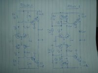
I’ve scribbled up my new topology Vs the old below. Figure A shows a simplified conventional symmetrical differential input stage and VAS. Each LTP has a tail current of 4.8mA, which divides evenly into each leg, giving a 2.4V drop across each 1k collector load resistor, RA and RB. The VAS transistors drop 0.7V each to give 1V across each 100 ohm VAS emitter degeneration resistor (RC and RD) and a quiescent VAS current of 10mA.
This topology is less than optimal because it doesn’t make use of the collector current swing in one leg of each LTP. Figure B shows the “Kleinschmidt” version. Each LTP is loaded with a current mirror and the quiescent 2.4V drop across the 1k collector load resistors RA and RB is restored by the inclusion of a pair of 2.4mA current sources.
We now have push-pull drive to the VAS, so the gain of each LTP is instantly doubled, and the 10mA quiescent bias setting of the VAS isn’t compromised.
So y’all see? - we don’t have of sacrifice our current mirrors when going symmetrical after all. Now am I a clever boy or what? I don’t know if anyone has come up with this before (I’ve certainly never seen it in all my years of audio fiddling) and I don’t know if it will take-off, but just remember y’all, that y’all seen it here first..........
Cheers,
Glen
I’m quite happy at having achieved what I set out to do, so I’ll quickly give y’all a quick run-down…….
I’ve scribbled up my new topology Vs the old below. Figure A shows a simplified conventional symmetrical differential input stage and VAS. Each LTP has a tail current of 4.8mA, which divides evenly into each leg, giving a 2.4V drop across each 1k collector load resistor, RA and RB. The VAS transistors drop 0.7V each to give 1V across each 100 ohm VAS emitter degeneration resistor (RC and RD) and a quiescent VAS current of 10mA.
This topology is less than optimal because it doesn’t make use of the collector current swing in one leg of each LTP. Figure B shows the “Kleinschmidt” version. Each LTP is loaded with a current mirror and the quiescent 2.4V drop across the 1k collector load resistors RA and RB is restored by the inclusion of a pair of 2.4mA current sources.
We now have push-pull drive to the VAS, so the gain of each LTP is instantly doubled, and the 10mA quiescent bias setting of the VAS isn’t compromised.
So y’all see? - we don’t have of sacrifice our current mirrors when going symmetrical after all. Now am I a clever boy or what?
I don’t know if anyone has come up with this before (I’ve certainly never seen it in all my years of audio fiddling) and I don’t know if it will take-off, but just remember y’all, that y’all seen it here first.......... Cheers,
Glen
Attachments
G.Kleinschmidt said:...
So y’all see? - we don’t have of sacrifice our current mirrors when going symmetrical after all. Now am I a clever boy or what?
Cheers,
Glen
Get back to my post (http://www.diyaudio.com/forums/showthread.php?postid=1173625#post1173625) where I have shown a symetrical input stage with current mirror loads which I think is more simple than your figure B. In fact I have seen this design (my post) first in 1985 from JLH.
If you could compare your figure B design with the input stage topology I have posted I think it would be beneficial for lots of peoples..
Of course this is more work to do...
fab said:
Get back to my post (http://www.diyaudio.com/forums/showthread.php?postid=1173625#post1173625) where I have shown a symetrical input stage with current mirror loads which I think is more simple than your figure B. In fact I have seen this design (my post) first in 1985 from JLH.
If you could compare your figure B design with the input stage topology I have posted I think it would be beneficial for lots of peoples..
Of course this is more work to do...
I did some simulations of the JLH topology back when I received you first post. It incorporates the VAS stage in a localised negative feedback loop, which heavily cuts back the VAS gain. This improves the VAS linearity, but the circuit only seems to be effective a giving a worthwhile improvement in linearity if the quiescent VAS current is either less or not a lot greater than the LTP tail current. For instance, in your circuit the LTP tail current is approximately 3.5mA while the VAS current is only 2mA.
This, in my opinion, makes the circuit a bit inflexible, because such a low VAS current compromises slew rate and driving ability.
Cheers,
Glen
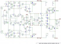
OK guys, here it (finally) is.......
I'm now working on a little +/-20V regulator for the low power rails.
http://users.picknowl.com.au/~glenk/classa.gif
I'm now working on a little +/-20V regulator for the low power rails.
http://users.picknowl.com.au/~glenk/classa.gif
An externally hosted image should be here but it was not working when we last tested it.
G.Kleinschmidt said:
I did some simulations of the JLH topology back when I received you first post. It incorporates the VAS stage in a localised negative feedback loop, which heavily cuts back the VAS gain. This improves the VAS linearity, but the circuit only seems to be effective a giving a worthwhile improvement in linearity if the quiescent VAS current is either less or not a lot greater than the LTP tail current. For instance, in your circuit the LTP tail current is approximately 3.5mA while the VAS current is only 2mA.
This, in my opinion, makes the circuit a bit inflexible, because such a low VAS current compromises slew rate and driving ability.
Cheers,
Glen
My post was only an example. I agree that 10ma VAS current is more appropriate for higher slew rate. See revised circuit with 10ma VAS (added buffer stage between input stage and VAS). The VAS gain is increased and high enough (at least for me). LTP current is about 4.5 ma (example again). In fact, you can use different current settings to your liking but select the proper resistor value.
Attachments
G.Kleinschmidt said:OK guys, here it (finally) is.......
I'm now working on a little +/-20V regulator for the low power rails.
http://users.picknowl.com.au/~glenk/classa.gif
It now looks more and more like my posted circuit (at least for the symetrical cascode VAS...)
How do you set the base voltage of Q23 and Q26 ...?
Borbely site provides some interesting high performance discrete regulator circuit schematics...
fab said:
My post was only an example. I agree that 10ma VAS current is more appropriate for higher slew rate. See revised circuit with 10ma VAS (added buffer stage between input stage and VAS). The VAS gain is increased and high enough (at least for me). LTP current is about 4.5 ma (example again). In fact, you can use different current settings to your liking but select the proper resistor value.
Yes, you can run a higher VAS current if you want. What I'm saying is that, in simulation, the linearity degrades a lot if the VAS current is too much higher than the LTP tail current. I tried buffering the VAS with an emitter follower, but it gave virtually nill improvement.
fab said:
It now looks more and more like my posted circuit (at least for the symetrical cascode VAS...)
How do you set the base voltage of Q23 and Q26 ...?
Borbely site provides some interesting high performance discrete regulator circuit schematics...
Hmmm...??.... The final schematic is the same as my first version, with the exception of the modified VA stages, which are now as per my 'Figure B' scheme outlined earlier. VAS current is set to approximately 10mA by the quiescent voltage developed across R22 and R25 by the symmetrical current source formed by Q3, Q4 and R7.
Cheers,
Glen
- Status
- This old topic is closed. If you want to reopen this topic, contact a moderator using the "Report Post" button.
- Home
- Amplifiers
- Solid State
- My new mini Class A amp.