C3//R3?
Glen,
I hope this is not too picky.
But, it seems to me that your input network (R2, C3//R3) will start to roll-off at ~13KHz. If you are my age; it probably doesn't matter!
Interesting circuit; thanks for sharing it and your developmental perturbations. I am sorry that you felt it necessary not to keep posted the intermediate circuits.
Best Wishes,
VSR
Re: C3//R3?
G'day sherelec.
Thanks for the compliments. C3 'sees' R2 in parallel with the series combination of R1, C1+C2 and the output impedance of the audio source. Unless driven from a source with an unusually high output impedance, the frequency roll off will be well above 200kHz. This is done to suppress RFI.
Cheers,
Glen
sherelec said:Glen,
I hope this is not too picky.
But, it seems to me that your input network (R2, C3//R3) will start to roll-off at ~13KHz. If you are my age; it probably doesn't matter!
Interesting circuit; thanks for sharing it and your developmental perturbations. I am sorry that you felt it necessary not to keep posted the intermediate circuits.
Best Wishes,
VSR
G'day sherelec.
Thanks for the compliments. C3 'sees' R2 in parallel with the series combination of R1, C1+C2 and the output impedance of the audio source. Unless driven from a source with an unusually high output impedance, the frequency roll off will be well above 200kHz. This is done to suppress RFI.
Cheers,
Glen
G.Kleinschmidt said:
Yes, you can run a higher VAS current if you want. What I'm saying is that, in simulation, the linearity degrades a lot if the VAS current is too much higher than the LTP tail current. I tried buffering the VAS with an emitter follower, but it gave virtually nill improvement.
Hmmm...??.... The final schematic is the same as my first version, with the exception of the modified VA stages, which are now as per my 'Figure B' scheme outlined earlier. VAS current is set to approximately 10mA by the quiescent voltage developed across R22 and R25 by the symmetrical current source formed by Q3, Q4 and R7.
Cheers,
Glen
Ok my last intervention on this thread. See http://www.ne.jp/asahi/evo/amp/J200K1529/report.htm figures 3, 4 and 5 for similar arrangement like yours (current mirror loads insym diff stage with VAS base voltage set by curent source...) since it may gives you more ideas...
Good luck

fab said:
Ok my last intervention on this thread. See http://www.ne.jp/asahi/evo/amp/J200K1529/report.htm figures 3, 4 and 5 for similar arrangement like yours (current mirror loads insym diff stage with VAS base voltage set by curent source...
Good luck
Link doesn't work!

G.Kleinschmidt said:
Link doesn't work!
I don't understand since I click on YOUR reply to my post and it works!
May someone else could confirm?
fab said:
I don't understand since I click on YOUR reply to my post and it works!
May someone else could confirm?
I get this:
The page cannot be displayed
There is a problem with the page you are trying to reach and it cannot be displayed.
--------------------------------------------------------------------------------
Please try the following:
Open the www.ne.jp home page, and then look for links to the information you want.
Click the Refresh button, or try again later.
Click Search to look for information on the Internet.
You can also see a list of related sites.
HTTP 500 - Internal server error
Internet Explorer
It could just be the ISP I'm on at the moment. I'll try from my computer at home tonight.
BTW, I didn't copy the idea from somwehere else, but I'll be surprised if it hasn't been done before, since it is so simple. That's part of the reason why I'm openly posting it here - to find out.
G.Kleinschmidt said:
I get this:
The page cannot be displayed
There is a problem with the page you are trying to reach and it cannot be displayed.
--------------------------------------------------------------------------------
Please try the following:
Open the www.ne.jp home page, and then look for links to the information you want.
Click the Refresh button, or try again later.
Click Search to look for information on the Internet.
You can also see a list of related sites.
HTTP 500 - Internal server error
Internet Explorer
It could just be the ISP I'm on at the moment. I'll try from my computer at home tonight.
BTW, I didn't copy the idea from somwehere else, but I'll be surprised if it hasn't been done before, since it is so simple. That's part of the reason why I'm openly posting it here - to find out.
Try http://www.diyaudio.com/forums/showthread.php?postid=1085387#post1085387 where it shows tha main "parent" link to the one I have posted. See "...2SJ200/2SK1529 link"
I got the link. The sublimeness of fully balanced topologies - I love it.
Some good ideas to overcome the points with this type of design raised by Glen at the start of the thread.
I tried this (but without specific circuitry to keep the VAS's in balance) about 2 years ago, and got great simulation results but not in practice. I will have to give it a try again.
One point to note is that the value of the VAS emitter degenration resistors is quite critical and linked to the VAS/LTP current ratios as someone already pointed out. Too high and you get a nasty kink in the bode plot (pole-zero pair? - someone help me out here).
I guess if you can get this fully balanced, current mirror driven VAS right, because of the f/back available, it may make distortion null circuity a bit supurfluous.
One question I have to ask though, is will the forced imbalance in the mirror not lead to increased distortion.
Look forward to your findings Glen.
Bonsai said:
One question I have to ask though, is will the forced imbalance in the mirror not lead to increased distortion.
Look forward to your findings Glen.
G'day Bonsai.
My 'figure B' circuit (post 14) doesn't effect the balance of the current mirror. In my final circuit (post 17) the currents from Q3 & Q4 only flow through R22 and R25. This establishes a quiescent voltage drop across R22 and R25 of 2.4V each, forcing a rather stable 10mA quiescent current in the VA stages. Consider the circuit node at the base of Q23. Q19 mirrors the collector current of Q12. In the quiescent state, Q19 ‘sources’ 2.5mA (half the LTP tail current) to the base of Q23, while Q11 ‘sinks’ 2.5mA from the base of Q23. The VAS biasing current from Q3 has nowhere else to flow, but through the VAS biasing resistor R22. R22 also forms the collector load for the LTP, establishing the stage gain in conjunction with the LTP's emitter degeneration resistors.
Cheers,
Glen
Bonsai said:Glen,
if R22 establishes the stage gain with the LTP emmiter degenration resistor, then surely you don't have a constant current load anymore - the gain is R22/(2*Rdegen)?
Thats right. But the current mirror does provide "push-pull" drive to the VAS, which effectively doubles the LTP's gain. The gain is equal to R22/Rdegen.
Cheers,
Glen
fab said:....the main "parent" link to the one I have posted. See ...2SJ200/2SK1529 link"
Here is the ' 2SJ200 - 2SK1529 link '
at that nice japan diy power amp website:
1. Schematics amp + power supply + pictures of power amp!
http://www.ne.jp/asahi/evo/amp/Dnfb/j200k1529.htm
2. Here is the DIRECT LINK to schematic image, for those interested:
http://www.ne.jp/asahi/evo/amp/Dnfb/exp4.gif
3. For gain control (~ 20), one JFET OP-Amp is used.
/Regards lineup
Glen, maybe take a look at Bob Cordell's front end design for further inspiration - clever DC feedback technique to keep the mirror in balance. I do not know if this will work on a fully balanced topology, but it might (load the VAS output to ground with resistor. R22 has to go!
Bonsai said:Glen, maybe take a look at Bob Cordell's front end design for further inspiration - clever DC feedback technique to keep the mirror in balance. I do not know if this will work on a fully balanced topology, but it might (load the VAS output to ground with resistor. R22 has to go!
Been there, done that! My second schematic in fact used a VAS similar to Bob's design, but it simply won't work in a symmetrical topology. The LTP DC gain is far too great, and even the slightest Ic imbalance in the LTP will either saturate its respective VAS or cut it off.
In the non-symmetrical topology, the VAS is typically loaded with a constant current source. The effect of DC negative feedback steers the VAS current in the quiescent state so that, regardless of any Ic imbalance in the LTP, the VAS current matches that of the constant current source, thus giving an output voltage of 0V (+/- a slight offset voltage).
In the fully symmetrical topology, unfortunately, we do not have the luxury of a fixed and stable constant current source load for each VA stage – each VAS transistor is in fact the current reference for the other and must be stable and predictable. In a symmetrical design, the gain of each LTP must be sufficiently low so that any Ic imbalance does not appreciably upset the quiescent VAS current. If this requirement is not met, you’ll likely end up with one VAS biased diametrically opposed to the other, such that the DC negative feedback will not be able to steer both to a stable quiescent state. This amplifier will just sit with its output swung hard against one of the rails.
Cheers,
Glen
fab said:
Try http://www.diyaudio.com/forums/showthread.php?postid=1085387#post1085387 where it shows tha main "parent" link to the one I have posted. See "...2SJ200/2SK1529 link"
Okaayyyy......I’m on my home computer now and I can access that page. I can’t read Japanese, but I can read schematic diagrams. That guy is using a rather different constant current source and a MOSFET VAS, but the biasing scheme is essentially identical in operation to what I have come up with for my BJT-VAS design.
Damn it!
 That’s yet another idea, which I now cannot ascribe my name to. Someone around here once pointed out that there is nuthin new in audio design.
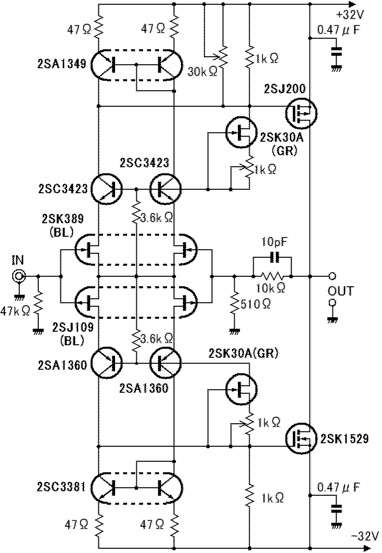
Glen, yep - been through the loop you mentioned in your last post as well.
One way might be to just run one half of the VAS at a slightly higher (lower) current to force it one direction and then let the DC loop keep theoutput centered. This way, the balance in the individual LTP pairs can be maintained (for minimal distortion.
One way might be to just run one half of the VAS at a slightly higher (lower) current to force it one direction and then let the DC loop keep theoutput centered. This way, the balance in the individual LTP pairs can be maintained (for minimal distortion.
Bonsai said:Glen, yep - been through the loop you mentioned in your last post as well.
One way might be to just run one half of the VAS at a slightly higher (lower) current to force it one direction and then let the DC loop keep theoutput centered. This way, the balance in the individual LTP pairs can be maintained (for minimal distortion.
Actually, all you need is a DC servo that monitors the average DC current through one VAS transistor, and steers its respective LTP to stabilize the quiescent VAS current. This servo-steered VAS will then become the current ‘reference’ for the other VAS stage, whose quiescent operating point will be steered to match the ‘reference’ by the DC negative feedback.
I was going to do this in my 12W design discussed here, but decided against it on grounds of complexity, as I only intended for this to be a relatively simple design. However, the compromise ‘Figure B’ circuit is a worthwhile improvement over the standard topology.
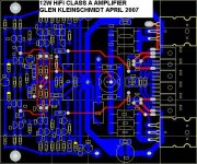
Boards are 80% complete
Cheers,
Glen
- Status
- This old topic is closed. If you want to reopen this topic, contact a moderator using the "Report Post" button.
- Home
- Amplifiers
- Solid State
- My new mini Class A amp.