I’ve been working on this test amp for a short time and thought I’d post the project. Here are a couple reasons for posting:
1) I’d like feedback from anyone who has used this assembly method (I first saw this construction method on www.ampslab.com) and may have advice or suggestions to make this perform.
2) If anyone hasn’t seen this before, maybe it will spur someone’s creativity or will serve as inspiration for someone who hasn’t built a project to start something. Feel free to let me know if this is the case too.
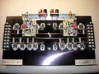
I’m building this system for a couple reasons. First is to test the large copper wire/power point-to-point/connected by terminal strips/power transistor construction method. I like the way it looks and it seems to be reasonable for prototypes and home-built equipment. It certainly wouldn’t fly for anything professional or commercial. So here is my first attempt using this technique and from the ease of implementation and flexibility so far, if it performs well, I’ll be using it again.
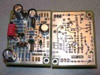
The next items I’m testing are the PCBs. They are basically Doug Self’s Blameless design. I used ExpressPCB’s standard size boards (2.5” x 3.8”, double-sided, through-hole plated) and put two complete amp driver circuits on each PCB. So this test system will allow me to validate the PCB design and get them dialed-in before I move on to my monoblock project (wait ‘til I post them some day – they’ll be beasts!).
The power transistors are TIP35C/36C (100V, 25A, 125W, NPN/PNP compliments) set up as darlingtons with TIP31C/32C. The slab of heatsink was purchased at the local HSC surplus store for $11.
My next step is to finish the transistor’s wiring, add bias transistors with wiring to the PCBs, finish input and output wiring, and of course add the power supply. I’ll provide more details and specs once this is done.
1) I’d like feedback from anyone who has used this assembly method (I first saw this construction method on www.ampslab.com) and may have advice or suggestions to make this perform.
2) If anyone hasn’t seen this before, maybe it will spur someone’s creativity or will serve as inspiration for someone who hasn’t built a project to start something. Feel free to let me know if this is the case too.
I’m building this system for a couple reasons. First is to test the large copper wire/power point-to-point/connected by terminal strips/power transistor construction method. I like the way it looks and it seems to be reasonable for prototypes and home-built equipment. It certainly wouldn’t fly for anything professional or commercial. So here is my first attempt using this technique and from the ease of implementation and flexibility so far, if it performs well, I’ll be using it again.
The next items I’m testing are the PCBs. They are basically Doug Self’s Blameless design. I used ExpressPCB’s standard size boards (2.5” x 3.8”, double-sided, through-hole plated) and put two complete amp driver circuits on each PCB. So this test system will allow me to validate the PCB design and get them dialed-in before I move on to my monoblock project (wait ‘til I post them some day – they’ll be beasts!).
The power transistors are TIP35C/36C (100V, 25A, 125W, NPN/PNP compliments) set up as darlingtons with TIP31C/32C. The slab of heatsink was purchased at the local HSC surplus store for $11.
My next step is to finish the transistor’s wiring, add bias transistors with wiring to the PCBs, finish input and output wiring, and of course add the power supply. I’ll provide more details and specs once this is done.
Attachments
Hi,
you did really well to fit a blameless into 2.8x1.9inch and leave room for screws and non-plated land.
The TIPs are a bit slow compared to the transistors Self used.
Stick with 1943/5200 or better.
Is that 4pair in each channel? That pushes Self's low impedance version into mediocrity.
Any chance of posting a detailed close up of both sides of your PCB?
If you go to no miller cap (JLH) compensation then leave pads for his other four compensation locations he has incorporated into his 80W mosfet design.
I’ll take some closer pictures tonight and post them. It wasn’t real tough to compress the design enough to fit 2.5” x 1.9”. The ExpressPCB CAD program is very easy to use and the circuit isn’t too complex. The PCB contains everything but the output stage and darlington pre-drivers and even has extra supply filtering.
I used the TIP35C/36C devices because I had a handful of each that I hadn’t used in ages plus I wanted to see how the Blameless circuit would perform with “typical” output devices. By typical, I mean nothing fancy, or ultra fast, or too linear.
As for using 16 devices, four-pair per channel, I wanted to test the capability of the copper wire construction and try to dump 20 amps into 1-ohm (400W). The devices should handle it and if everything goes well, the PCB design and construction method should prove to be robust enough for future projects.
Hi,
4pair might just manage this, but that current might blow the drivers, particularly if the gain of the TIPs is low, or very low at peak current.try to dump 20 amps into 1-ohm (400W).
Attached is a close-up picture of the PCA I designed. The open pads to the right (of the PCB showing components) are for the bias transistor and resistors. There are also a couple extra pads in case I have to add additional feedback caps for stability, but hopefully I won’t need them. I made both the top and bottom full ground planes with a full, common grounds because the entire PCA will be a single low-current ground point. Maybe a mistake; we’ll see.
The TO-92 devices are MPS8099 and MPS8599 and the two Class ‘A’ transistors are MPSU07 and MPSU57. Again, not the best devices but they’re adequate for testing.
Regarding the TIP devices delivering 20 amps, I don’t see a problem. Each is rated 25A continuous and 40A peak, hFE is 25 minimum, and there are four paralleled. Anyway, this too will be proven upon testing.
Attachments
Hi,
What is the TIP gain@ 5A?
Now look at the base current that the driver has to supply.
Ib=Ic/hFE =20/25 = 0.8A
Next look at driver dissipation into a reactive load.
Assume that the Driver Vce=+Vrail and driver Ic=0.8A the Pdriver=30V*0.8=24W. What does the datasheet say?
Could the Vrail be higher than 30V? if the load is taking 20A then the rail voltage could be much higher.
4pair delivering 20A (peak or rms?) is 5A per device.TIP devices delivering 20 amps, I don’t see a problem. Each is rated 25A continuous and 40A peak, hFE is 25 minimum
What is the TIP gain@ 5A?
Now look at the base current that the driver has to supply.
Ib=Ic/hFE =20/25 = 0.8A
Next look at driver dissipation into a reactive load.
Assume that the Driver Vce=+Vrail and driver Ic=0.8A the Pdriver=30V*0.8=24W. What does the datasheet say?
Could the Vrail be higher than 30V? if the load is taking 20A then the rail voltage could be much higher.
- Status
- This old topic is closed. If you want to reopen this topic, contact a moderator using the "Report Post" button.