Hello to all. As a newcomer to the DIYaudio, i am little afraid and ask your comprehension for this. Sorry to my bad English. I see here that you discuss for the NFB. According to my humble opinion, this is not as bad as many they believe. On the contrary, it offers the biggest stability in the amplification arrangement. Of course, if we do not take under aspect certain things in her application, the result is indeed ugly. And i see here that you discuss for these things. According to my observations, it should we are careful about two factors. In the NFB the feedback at rule is 100% and the voltage divider that controls the closed loop gain is coupled with the A.C. mode to the GND loop. The problem here, is the electrolytic capacitor via which is achieved the A.C. coupling. He mainly is responsible for the phase shifts at low frequencies. This problem is resolved, if we increase the capacity at least above from 470 ìF. An optimum value is 1000 ìF, but now comes the problem of size as a capacitor with such capacity and with working voltage at 100 V.D.C. it is very big. If we see the work of many designers today, they resolve this problem with an intelligent trick. By placing a capacitor at 1000 ìF but with working voltage at 16 V.D.C. – a such is of course small in volume - and in order to protect him from the high excursions of signal, clamping it with two or four diodes back to back connected. The other factor is the phase shifts at higher frequencies. This caused from the series resistor, rather than from the shunt resistor of voltage divider. If we see the input subtracter- or differential amplifier, or long tailed pair- the shunt resistor of the input transistor of the pair, has the same value with the series resistor of the output transistor, to get the same gain and keeping a balance in collector currents avoiding thus the D.C. offset in output. As i believe, because the b-e impedance of each transistor then changed, in sequence there is a change and in the hfe parameters of the input quadrapole, thus caused the phase shift at higher frequencies because the time lag in the transistor of the pair that sees the output. And this problem resolved from many designers, by putting a bypass branch comprised by an R-C network around the series resistor – some bootstrapping it is offered thus. Because my long experience about P.A. sound reinforcements, as i have seen so many years, the vast majority of designers in power amplifiers uses this scheme of NFB, as the stability and durability is the first criterion here. They would be precious and your opinion on this, as i use also this scheme in my trial designing of a power amplifier.
Hi,
Welcome to the forum.
There are many opinions here of NFB.
NFB opinions are a religion to many here
Thank you for your insight.
Welcome to the forum.
An externally hosted image should be here but it was not working when we last tested it.
There are many opinions here of NFB.
NFB opinions are a religion to many here
Thank you for your insight.
problem to upload images
Sorry but i can’t to upload two very informative schematic diagrams. Thus if you want to take a better idea than what i say, you must visit my web page at http://www.eal.gr
Sorry but i can’t to upload two very informative schematic diagrams. Thus if you want to take a better idea than what i say, you must visit my web page at http://www.eal.gr

i hope this time the images quoted
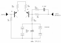
In order to understand better the arrangement, i quote a practical circuit below. Q1 and Q2 form the usual differential amplifier or long tailed pair; with other words they constitute a subtracter to reject the errors from the output via the NFB branch. R5 and R6 constitute the voltage divider that fixes the voltage gain of overall circuit and in this case is: Av = R5/R6 = 46,15. R2 and R3 are the transconductance degeneration resistors as the collector of Q1 translates the input voltage to an equivalent current that it drives the base of VAS. C2 is the element that allows the A.C. coupling of NFB branch to GND and thus is achieved 100% feedback. The four diodes clamp the voltage excursions to a max value 2 X 0,7V = 1,4V and thus the smaller in volume C2 but with large capacity can be used to resolve the L.F. phase shift problem. I have examined thoroughly that, by applying a 100 Hz square signal in the input and observing the output with the scope. As long as it grows the capacity of C2, so much minimizes the tilt from the rising to the falling edge of the square signal at output. R4 and C1 constitute a speed up network around the series resistor R5 and it has the same value with the shunt resistor R1 to balance the collector currents of Q1 and Q2. This small network restores the phase shift at higher frequencies.
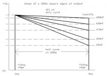
And in the second figure you can observe different tilts of a square signal with different capacities of C2.
One still observation that i have to make, is that this subject it has also relation with the transient response in L. F. When i dealt with this for first time, discovered that i had wrong, as i still believed –as many –that this has relation with the size of the power supply electrolytic capacitors. As long as bigger are these so much better response in low frequency material. With surprise i discovered that the increase of capacity of the A.C. coupling capacitor it had much bigger effect in this.
In order to understand better the arrangement, i quote a practical circuit below. Q1 and Q2 form the usual differential amplifier or long tailed pair; with other words they constitute a subtracter to reject the errors from the output via the NFB branch. R5 and R6 constitute the voltage divider that fixes the voltage gain of overall circuit and in this case is: Av = R5/R6 = 46,15. R2 and R3 are the transconductance degeneration resistors as the collector of Q1 translates the input voltage to an equivalent current that it drives the base of VAS. C2 is the element that allows the A.C. coupling of NFB branch to GND and thus is achieved 100% feedback. The four diodes clamp the voltage excursions to a max value 2 X 0,7V = 1,4V and thus the smaller in volume C2 but with large capacity can be used to resolve the L.F. phase shift problem. I have examined thoroughly that, by applying a 100 Hz square signal in the input and observing the output with the scope. As long as it grows the capacity of C2, so much minimizes the tilt from the rising to the falling edge of the square signal at output. R4 and C1 constitute a speed up network around the series resistor R5 and it has the same value with the shunt resistor R1 to balance the collector currents of Q1 and Q2. This small network restores the phase shift at higher frequencies.
And in the second figure you can observe different tilts of a square signal with different capacities of C2.
One still observation that i have to make, is that this subject it has also relation with the transient response in L. F. When i dealt with this for first time, discovered that i had wrong, as i still believed –as many –that this has relation with the size of the power supply electrolytic capacitors. As long as bigger are these so much better response in low frequency material. With surprise i discovered that the increase of capacity of the A.C. coupling capacitor it had much bigger effect in this.
Attachments
Hi Fotios,
re, the graph showing slope on the 100Hz square wave top.
Are those capacitor values for the same 390r resistor?
I would have chosen 330uF (RC=0.130S) to give a 1 to 1.5Hz F-3 turn over frequency. I also include a high pass input filter set to about 90mS.
I do not recall seeing even a 20Hz signal with that amount of slope. I am surprised at the results you have obtained.
Are you rolling off the bass response with another high pass filter?
AndrewT said:Hi Fotios,
re, the graph showing slope on the 100Hz square wave top.
Are those capacitor values for the same 390r resistor?
I would have chosen 330uF (RC=0.130S) to give a 1 to 1.5Hz F-3 turn over frequency. I also include a high pass input filter set to about 90mS.
I do not recall seeing even a 20Hz signal with that amount of slope. I am surprised at the results you have obtained.
Are you rolling off the bass response with another high pass filter?
Hi and in you Andrew T (somehow thus greet the people in my country)
From as long as i understand you are also a measurement fan as i. However it should not we are so dogmatic. The graph that i present is simply indicative – something that appears moreover from the vertical axis Vp where not written values anywhere – and my aim is to emphasize something important that do not know many others - to my big surprise! Do not believe that this subject is my trial discovery. I read the book of Douglas Self “Audio Power Amplifiers” before five years – if you have not made already this, read it because is very interesting book – and in all his drawings he appeared this big capacitor. Up to then i used capacitors of 100ìF, and thus i began to experiment with bigger capacities so that i verify their value, as Self does not argue their usefulness nowhere in his book. What i wrote it is true but i do not believe you took the rule and measured the distance of subdivisions in the vertical axis! Actually a slope from the other abstain a few milliVolts. Thus if i drew him as it is actually would need a magnifying lens in order to distinguish between them! I hope you understood that the reason was clearly practical. What has importance is that this small differences in the tilt of square wave they are translated in improvement of coupling of feedback circuit in low frequencies. And be certain – in hearing test has been verified this – that it is related with the improvement of the transient response of amplifier in low frequency passages. I know that it is heard curious, but it is fact, at least in my amplifier. The resistor value is indeed constant at 390 Ù as you ask and has relation with the input sensitivity of the amplifier which is 1 Vrms for full output swing. It cannot change, because the resistors of 18KÙ has relation with the input impedance (50KÙ) and the transistors; that are of type MPSA56 or 2N5401 (Vce = 80/150Vdc – Ic = 0,5A). In any case i could not understand what you want to say there that you report “high pass input filter set about 90ms”. Where you place this filter? Ét is easy you include a diagram in order to i understand better? If you want, i have not objection to send you the complete circuit of amplifier, but personally in you, because i do not want to publish it.
just a question..... you are trying to get 100% feedback? this would set the gain at unity. dc gain should be unity to minimize offset, ac gain can be whatever you need, unity for a buffer amp, or more for a power amp.
i kind of prefer to use separate feedback loops for dc and ac, using a dc servo to eliminate offset, and a simple resistive voltage divider for the ac. i also try to eliminate the integrating capacitor from the feedback loop, and instead use frequency compensation elsewhere, such as in the predriver or driver stage. the proper way to compensate the amp is to change the phase response, rather than alter the feedback slope. i try to keep reactive components out of the feedback loop, since they tend to cause more problems than they solve. that's my opinion on feedback, and there are many who, for simplicity put capacitors in the feedback loop, and it works fine, and there are many wonderful amps out there that have them, but i prefer not to. i am also one of the people here who are perfectly happy with using NFB, both global and local. NFB is one of the most useful principles of electronics. all forms of signal processing would be impossible without it, and we would also have probably never got beyond the spark-gap and vacuum triode stage of electronic technology without it.
i kind of prefer to use separate feedback loops for dc and ac, using a dc servo to eliminate offset, and a simple resistive voltage divider for the ac. i also try to eliminate the integrating capacitor from the feedback loop, and instead use frequency compensation elsewhere, such as in the predriver or driver stage. the proper way to compensate the amp is to change the phase response, rather than alter the feedback slope. i try to keep reactive components out of the feedback loop, since they tend to cause more problems than they solve. that's my opinion on feedback, and there are many who, for simplicity put capacitors in the feedback loop, and it works fine, and there are many wonderful amps out there that have them, but i prefer not to. i am also one of the people here who are perfectly happy with using NFB, both global and local. NFB is one of the most useful principles of electronics. all forms of signal processing would be impossible without it, and we would also have probably never got beyond the spark-gap and vacuum triode stage of electronic technology without it.
Dear friend unclejed613unclejed613 said:just a question..... you are trying to get 100% feedback? this would set the gain at unity. dc gain should be unity to minimize offset, ac gain can be whatever you need, unity for a buffer amp, or more for a power amp.
i kind of prefer to use separate feedback loops for dc and ac, using a dc servo to eliminate offset, and a simple resistive voltage divider for the ac. i also try to eliminate the integrating capacitor from the feedback loop, and instead use frequency compensation elsewhere, such as in the predriver or driver stage. the proper way to compensate the amp is to change the phase response, rather than alter the feedback slope. i try to keep reactive components out of the feedback loop, since they tend to cause more problems than they solve. that's my opinion on feedback, and there are many who, for simplicity put capacitors in the feedback loop, and it works fine, and there are many wonderful amps out there that have them, but i prefer not to. i am also one of the people here who are perfectly happy with using NFB, both global and local. NFB is one of the most useful principles of electronics. all forms of signal processing would be impossible without it, and we would also have probably never got beyond the spark-gap and vacuum triode stage of electronic technology without it.
Your observations are right and supplement substantially certain gaps in my first post. Moreover this was also his aim, to learn from the knowledge of other. As you see in all other replies, simply they put questions and do not propose something different, up to moment you only make this. Our opinions converge, and i am very glad for your meeting. Would be very instructive a practical diagram what you say, because a picture deserves thousand words as we know. This i made moreover also in my next posts as you can see. It should not we forget that here it is a forum for the exchange of knowledge between us and not a tribune where we declaim.
- Status
- This old topic is closed. If you want to reopen this topic, contact a moderator using the "Report Post" button.
- Home
- Amplifiers
- Solid State
- the NFB and the time lag in L.F. and H.F.