Improved version of my HF0K6
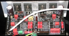
This is my new attempt to decrease the rise time - or to increase the intrinsic+extrinsic slew rate as like many people - with myself sticked in the single LTP pair in input - i know that the symetrical LTPs in input can provide a lower rise time by 30% at least thus a greater slew rate - by replacing the input stage transistors with Toshibas instead OnSemi according to the advice and the gift (40 pairs of complementary Toshibas!!!) of my good friend from WALES "aandy", the advice of my good friend "sandyK" from Australia to replace all ceramic caps with silvered mica, and finally to the advice of the very polite J. Curl for the foil caps.
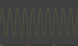
Well, from 2ìs the rise time had droped at 1,47ìs! I promise to post some curves - as usually and not only numbers - in the next days.
In general this project it is:
A class A/B amp. but with an increased iddle current at 50mA per output device.
A supply level of +/-60Vdc giving a power of 190W/8Ù (20-20000Hz).
A mix of Toshibas and OnSemis bipolars at whole; not FETs!
A THD+noise so small, that i can't measure it with my poor means for measurements.
The same for IMD.
A killing bass reproduction as in my previous model.
An improvement in mid-high reproduction by 100%. The Toshibas and the caps make the difference!
Current mirrors and CCS in all of the input stage.
Tripple darlington configuration in output with EF topology.
Non inductive parts - as soon as possible - in whole circuit, such as metal film resistors yet in 3W, metal oxide and metal plate resistors (a gift from FUTABA to me- many thanks LIVY!!).
Many thanks also to the carefull design of PCB. You may look at the symmetry of tracks, the thickness and nainly the ROUNDED corners. From my experience, a nice circuit can be destroyed from a bad layout drawing!
My better greetings in my friend Lineup who don't reply in my e-mail, and that if this project had implemented with symetrical input stage - that means with double LTP pairs - then the bandwidth may can touch the 250KHz (-3dB). Instead with its simple LTP it touches the 180KHz (-3dB). I promise documents in next days.
The architecture of this project it is almost the same with my project "Dirty Harry". This is the benefit of using current mirrors and constant current sources. The same framework for different power or quality amplifiers by substituting only few resistors and multiplying the output transistors, and changing the power supply level.
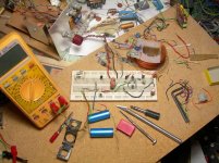
All the PCB hardwork is maden at MY HOME.
Below are the first photos
This is my new attempt to decrease the rise time - or to increase the intrinsic+extrinsic slew rate as like many people - with myself sticked in the single LTP pair in input - i know that the symetrical LTPs in input can provide a lower rise time by 30% at least thus a greater slew rate - by replacing the input stage transistors with Toshibas instead OnSemi according to the advice and the gift (40 pairs of complementary Toshibas!!!) of my good friend from WALES "aandy", the advice of my good friend "sandyK" from Australia to replace all ceramic caps with silvered mica, and finally to the advice of the very polite J. Curl for the foil caps.
Well, from 2ìs the rise time had droped at 1,47ìs! I promise to post some curves - as usually and not only numbers - in the next days.
In general this project it is:
A class A/B amp. but with an increased iddle current at 50mA per output device.
A supply level of +/-60Vdc giving a power of 190W/8Ù (20-20000Hz).
A mix of Toshibas and OnSemis bipolars at whole; not FETs!
A THD+noise so small, that i can't measure it with my poor means for measurements.
The same for IMD.
A killing bass reproduction as in my previous model.
An improvement in mid-high reproduction by 100%. The Toshibas and the caps make the difference!
Current mirrors and CCS in all of the input stage.
Tripple darlington configuration in output with EF topology.
Non inductive parts - as soon as possible - in whole circuit, such as metal film resistors yet in 3W, metal oxide and metal plate resistors (a gift from FUTABA to me- many thanks LIVY!!).
Many thanks also to the carefull design of PCB. You may look at the symmetry of tracks, the thickness and nainly the ROUNDED corners. From my experience, a nice circuit can be destroyed from a bad layout drawing!
My better greetings in my friend Lineup who don't reply in my e-mail, and that if this project had implemented with symetrical input stage - that means with double LTP pairs - then the bandwidth may can touch the 250KHz (-3dB). Instead with its simple LTP it touches the 180KHz (-3dB). I promise documents in next days.
The architecture of this project it is almost the same with my project "Dirty Harry". This is the benefit of using current mirrors and constant current sources. The same framework for different power or quality amplifiers by substituting only few resistors and multiplying the output transistors, and changing the power supply level.
All the PCB hardwork is maden at MY HOME.
Below are the first photos
An externally hosted image should be here but it was not working when we last tested it.
An externally hosted image should be here but it was not working when we last tested it.
dudaindc said:
Nice boards (as usual) Fotios.
I look forward to more construction details.
Thanks for sharing the results of your experiments.
Thanks for your kind words.
Your reply it gives me courage to continue against the difficulties that i confront in my daily life.
Thanks again
Fotios
hienrich said:very tasty work there Fotios............
are you using the 2SC2240/2AS970 pairs.......on your symetrical diff part of these amps?
")
cheers
Thanks hienrich.
Yes, you guess right. A total description of devices used is:
1) 2SC2240 - 2SA970
2) MJE15030 - MJE15031
3) MJL3281 - MJL1302
4) MJL21193 - MJL21194
5) MPSA06 - MPSA56
All resistors are metal film, except the emitter resistors which are metal plate and the zobel resistor which is a special fire proof metal oxide film resistor. There is not any inductive part at whole.
All caps in pF range are Cornell-Doubilier silvered mica.
All caps in nF range are WIMA polypropylene MKP type.
The only 3 electrolytics are Panasonic ECA type for audio use.
The big input dc blocking cap it is SCR silvered foil MKP.
Fotios
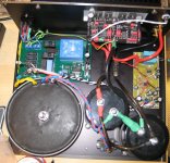
smithy666 said:Here is my latest project, a subwoofer amp for a Scanspeak 23W sub, using an Aussie Amplifiers NS150 module. Crossover is the Borbely All-FET, xover at 100Hz. The other amps are Stochinos.
First pic is the finished module
Hi smithy
Nice circuit. And above all, the parts you are using are of first quality as i can see.
My compliments sir!
Fotios
smithy666 said:Hi again Fotios
Likewise to you - very nice boards & construction. I really like seeing other people's boards/construction, as it always gives ideas for the next project
Best regards
smithy
Many thanks my friend.
During this time i am in the process of drawing the power supply board, including also the protection computer. It is a big board. For this reason i have not posted curves yet, because untill now the module supplied from my Lab power supply. When the project completed, then i will post the curves.
Regards
Fotios
Nice one, Bonsai
Here: http://www.diyaudio.com/forums/attachment.php?s=&postid=1134058&stamp=1171370431
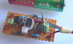
My own picture shows a small solid state devices.
Think nobody can guess what it is .........
Discrete & symmetrical, as usual from my Lineup Audio Lab.
Battery for compare of actual size.
Attachments
lineup said:
Nice one, Bonsai
Here: http://www.diyaudio.com/forums/attachment.php?s=&postid=1134058&stamp=1171370431
My own picture shows a small solid state devices.
Think nobody can guess what it is .........
Discrete & symmetrical, as usual from my Lineup Audio Lab.
Battery for compare of actual size.
Hi Lineup
It is a discrette operational amplifier for use in preamplifiers?
The only that i can say with certainty, is that it is not implemented with symmetrical LTPs as you like usually.
Greetings from Hellas
Fotios
fotios said:Hi Lineup
It is a discrette operational amplifier for use in preamplifiers?
Greetings from Hellas, Fotios
No.
It is symmetrical alright. But not a differential pair ....
For use in pre amplifiers, yes.
lineup said:
No.
It is symmetrical alright. But not a differential pair ....
For use in pre amplifiers, yes.
Then you are using two complementary transistors to share the input, which in sequence drive two complementary output transistors. Obviously, you are not using LTP configuration in feedback. Also the feedback it is DC coupled in GND, giving thus a low feedback ratio to obtain a wideband response.
Am i right now?
Fotios
Okay.
One NPN + one PNP put together, for temp compensation only.
This circuit is a discrete Symmetrical Shunt diode.
Each diode make 7.50 Volt from middle = 0 Volt.
To use this, you fead this symmetrical mirrored two VBE Multipliers
from two 9 VDC battery, with middle = 0 Volt.
As with shuntdiodes (zener) you have to put resistor to provide current into shunt.
Say 2 x 9.0 VDC input and 2 x 7.50 VDC output.
Makes 9.0-7.5 = 1.50 Volt drop.
Fead this symmetrical zener from two 1k5 resistors. 1 mA will flow through those VBE multipliers.
This one is not used as 2 x 7.50 Volt shunt regulator.
It is used for making 2 x 7.50 symmetrical Reference Voltages.
For my pre amplifier circuit.
lineup said:Okay.
One NPN + one PNP put together, for temp compensation only.
This circuit is a discrete Symmetrical Shunt diode.
Each diode make 7.50 Volt from middle = 0 Volt.
To use this, you fead this symmetrical mirrored two VBE Multipliers
from two 9 VDC battery, with middle = 0 Volt.
As with shuntdiodes (zener) you have to put resistor to provide current into shunt.
Say 2 x 9.0 VDC input and 2 x 7.50 VDC output.
Makes 9.0-7.5 = 1.50 Volt drop.
Fead this symmetrical zener from two 1k5 resistors. 1 mA will flow through those VBE multipliers.
This one is not used as 2 x 7.50 Volt shunt regulator.
It is used for making 2 x 7.50 symmetrical Reference Voltages.
For my pre amplifier circuit.
Well, this is a realy new and very smart invention.
What can i say then?
My compliments sir!
I asked your colaboration in building a preamplifier. If you are interested, give me a link to contact with you privatelly.
Greetings
Fotios
- Home
- Amplifiers
- Solid State
- Post your Solid State pics here