Hi All!
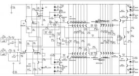
I'm simulating a Full Balanced Bridge, circuit and on the simulation program it seems to work very well: it recalls to the Ampzilla III but without all the auxiliary circuits around it, the only additional trimmer which is present, excluding the 2 that set the idle condition, is that on the base to ground connection of one of the input bias generator transistor. Chaning the current which flows in the Zener it allows a precise adjustment of the output DC level on both the halves.
I already done the layout for this and I'd like to get some comments and suggestions from You before putting it under the UV lamp")
Thank You Very Much
I'm simulating a Full Balanced Bridge, circuit and on the simulation program it seems to work very well: it recalls to the Ampzilla III but without all the auxiliary circuits around it, the only additional trimmer which is present, excluding the 2 that set the idle condition, is that on the base to ground connection of one of the input bias generator transistor. Chaning the current which flows in the Zener it allows a precise adjustment of the output DC level on both the halves.
I already done the layout for this and I'd like to get some comments and suggestions from You before putting it under the UV lamp
Thank You Very Much
Attachments
Hi
It looks like a pretty good classical circuit, I see no obvious flaw.
I'd just make some "economic" improvements: the three bias strings of each rail could be merged without inconvenient (perhaps adjust R5/7 to the new voltage, or add two diodes to the string). I'd also add a decoupling cap across the strings.
Note that you could retain your adjustment principle, as a minor voltage alteration of the cascode bias would have no effect.
LV
 nice
niceHi,
a red LED could replace each of the three diodes strings.
I, personally, don't like Miller compensation caps across the VAS. I suggest you reduce or remove the 22pF caps and add other compensation to adjust stability. Stability cap from VAS collector to inverting input (base) does the job and arguably sounds nicer.
I note your global feedback returns to the LTP emitters. Does this simulate well? I have no experience of this.
Do the junctions of r35 r36 and r45 r52 need to connect to ground? a single 13k would do the job.
The mpsa at the front end are relatively low gain and this will increase the input offset current. Consider high gain or even very high gain in these locations.
The closer the gain of the NPN and PNP the less the offset current. There is an argument that the NPN/PNP should not be equal so that the offset is always "one way" rather than moving either side of zero as junction temps (and gains) change under loading.
AndrewT,
I agree with You about the use of different components, Led and High gain Transistors and especially about the last ones, but I have many of them in house and prototyped with them
Also the use of a common resistor for the VAS cascode bias generator is a good choice: i'l do that.
From he simulation point of view (circuit maker) i see no issues, and the feedback going to the LTP is not an issue: this is how the true balanced bridge should work, look ad the Ampzilla III schema and on some books.
Thanh,
from what I remember the primary objective of a balanced equipment is not to lower the level of the harmonics but to have a better noise performance: however it seems to be in the simulation a little reduction in the 2nd and the other even harmonics if compared to the single ended version from which i started over to get this
- Status
- This old topic is closed. If you want to reopen this topic, contact a moderator using the "Report Post" button.