fab said:
In addition, I have found the Elektor schematics and read some thread about it.
I think my design has some differences
(no hi gain intermediate VAS stage but bootstrapped input stage, gain of 2 in output CFP stage, drain resistors including separate CFP feedback dividers for positive and negative, lower overall feedback) and I hope it will be less prone to oscillation.
Yes, I agree.
The Elektor has got exactly same basic idea for the output stage.
Bipolar driving MOS in CFP.
But as you say, there are many differences, if looking at total amplifier
and all the details of circuit.
And most transistors are different. Which is essential.
Re: New revised version 0E9
Hi,
this amplifier looks good, and I generally agreed with ilimzn. The only think I don't believe, is the buffer stage into the CFP stage. This amplifier will produce about 200W/8ohms, with 40V outout. What power will be dissipated on R80-82, and R101??? 40V/20ohms means 2A, and 80W dissipation...
sajti
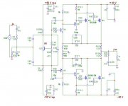
fab said:Here it is
I have followed most ilimzn advises but I am still waiting some responses to my last questions.
The amp was too slow, I needed to change compensation cap in differential stage.
I realised that without the bootstrap caps it the feedback may be too low...so I pout 220u at this time (but could be reduced if power-up thump...). Since the feedback was too high and I wanted a flat open loop frequency (audio) response I had to reduce the "natural" input stage gain. So now the feedbcak factor is about 40db. The local feedack output stage gain is now 2.
For now I will put aside the intermediate buffer in the CFP...
I understand that the VBE multiplier should be on same heatsink as the CFP bjt drivers but normally I use separate heatsink for N and P bjt drivers...what could I do?
Please comment.
Hi,
this amplifier looks good, and I generally agreed with ilimzn. The only think I don't believe, is the buffer stage into the CFP stage. This amplifier will produce about 200W/8ohms, with 40V outout. What power will be dissipated on R80-82, and R101??? 40V/20ohms means 2A, and 80W dissipation...
sajti
sajti said:
Hi,
this amplifier looks good, and I generally agreed with ilimzn. The only think I don't believe, is the buffer stage into the CFP stage. This amplifier will produce about 200W/8ohms, with 40V outout. What power will be dissipated on R80-82, and R101??? 40V/20ohms means 2A, and 80W dissipation...
sajti
Hi sajti,
I also thought about the high power in the CFP feedback divider this morning . Thanks for confirming that. The bad news is that to increase this divider ohmic value enough and keep the low feedback gain of the CFP to 2 (to ease stability as recommended by ilimzn), I wil need to increase substancially the R44-R45 resistor value (to avoid modulating the gain of the CFP with laod value) which will then decrease the mosfet drive current.
I have previously asked if I could use a lower drive current in the common source compared to the common drain (where a high current is required because of capacitance issue) but I got no response yet from anybody....If it is the same requirement then I will have to consider using the extra buffer (previous post 18 at http://www.diyaudio.com/forums/showthread.php?postid=1100006#post1100006 ) between the Q34 (Q35) and the associated mosfets...unless someone finds an alternate solution....
Please comment.
fab said:
I have previously asked if I could use a lower drive current
...
If it is the same requirement then I will have to consider using the extra buffer
.
For good driving on MOSFET laterals or hexfet,
we take the capacitance of the mosfet as a hint.
This would make me decide how low CURRENT ( which you ask about )
I could possible get away with.
I wouldn't complicate you amplifier using some extra buffers in output stage.
Go back to what you had first, fab, please!
For These laterals we have 600 / 900 pF ( see Lateral table in my attachment in prev. post ).
I have my own formula.
Actually 2 formulas.
================================================
A) This one is for make sure good driving. High Quality!
Current( mA ) = Ciss( pF) / 50
B) This formula is what will in most cases work.
This has been shown in other amplifiers before.
Current( mA ) = Ciss( pF ) /100
================================================
Using lineup formula A)
we get 12 mA / 18 mA, so we use ~ 18-20mA
Using lineup formula B)
we get 6 / 9 mA, so we use like 9-10 mA to drive SJ49/SK134
Regards
lineup
----
fab
PS. I don't know why I still help and post in this topic
I could do better spend my time in other threads
you have your best helper ilimzn
so what do you need me to disturb, anymore .....
lineup
lineup said:
For good driving on MOSFET laterals or hexfet,
we take the capacitance of the mosfet as a hint.
This would make me decide how low CURRENT ( which you ask about )
I could possible get away with.
I wouldn't complicate you amplifier using some extra buffers in output stage.
Go back to what you had first, fab, please!
For These laterals we have 600 / 900 pF ( see Lateral table in my attachment in prev. post ).
I have my own formula.
Actually 2 formulas.
================================================
A) This one is for make sure good driving. High Quality!
Current( mA ) = Ciss( pF) / 50
B) This formula is what will in most cases work.
This has been shown in other amplifiers before.
Current( mA ) = Ciss( pF ) /100
================================================
Using lineup formula A)
we get 12 mA / 18 mA, so we use ~ 18-20mA
Using lineup formula B)
we get 6 / 9 mA, so we use like 9-10 mA to drive SJ49/SK134
Regards
lineup
----
lineup
Thanks but since my mosfet needs about 0.75 VDC gate voltage to have 220 ma (total for the pair) bias, to get 10 ma it takes 75 ohms and this is my actual value! Therefore, I still have the problem of the CFP divider ohmic value that is too low when high output signal. I would like to avoid the extra buffer but how?...
lineup said:
fab
PS. I don't know why I still help and post in this topic
I could do better spend my time in other threads
you have your best helper ilimzn
so what do you need me to disturb, anymore .....
lineup
I value everybody comment and I am glad that you participate that much so please continue.... unless you think this thread is not worthy
fab said:
Thanks
but since my mosfet
needs about 0.75 VDC gate voltage to have 220 ma (total for the pair) bias,
to get 10 ma it takes 75 ohms and this is my actual value!
Therefore, I still have the problem of the CFP divider ohmic value that is too low when high output signal.
I would like to avoid the extra buffer but how?...
And at some real output maybe these MOSFET have VGS = 1.5 Volt
So we end up with 20mA across 75 Ohm resistors.
This is well in line with my both formulas,
that came up with A) 18-20mA, B) 9-10mA.
Who ever decided 75 Ohm has got about same idea, like lineup, what it takes to drive ONE of these MOSFET.
For driving TWO in parallel
I would probably use two 75 Ohm in parallel.
Or in other words, I would lower R44 to 47 Ohm
---------------------
How do you solve the resistance values in CFP feedback?
I usually does this:
Try to figure out the situation at a certain high output level.
And see if that works.
A hint:
In these type of output stages,
it is important for good result
to allow such HIGH GAIN, that the local feedback will NOT be TOO LOW!
We have to allow a proper amount of Feedback.
This is most important when LOAD is maximum HEAVY: say 3-4 Ohm.
I have seen this when using same configuration using BJT output devices.
The same considerations goes for so called 'Current Feedback Amplifiers'.
you can search the web or This Forum and see some info of wellknown 'Current feedback' amplifiers.
-------------------------------------
What decides the gain in this output stage?
I will now refer to your schematic:
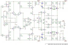
Posted 2007-01-07, 'amp_fab_novas_0e2simple.jpg'
See my attachment.
Look at Q34 and 2SJ49 and the load 4 Ohm.
----------------------------------
Roughly speaking
Gain in Q34 is: R44 / R80 = 7.5
Gain in 2SJ49 is:
Load 4 Ohm / R54 (0.18 Ohm) = ~20
Total Gain ~ 150
Actually there are other things that will lower this.
I think for example RDS of 2SJ49 and load variations, going down to 2.5-3 Ohms.
We can increase this gain, by lowering R80 and R54 further.
But the drawback will be: worse control of bias level in output.
We use some resistances to set the idle bias
and make sure it stays within reasonable level when the amplifier is in operations.
About Q34 + Q35. They do an important job.
They are the LINK between VAS stage and Output stage.
I would use drivers that work well at 50-100mA.
This will also allow rather high currents and Low values for R44 and R80.
And good if Q34/Q35 they have Rather high Gain, HFE
Candidates, as usual:
BD139 / BD140 ( TO126 ), higher gain
MJE15030 / MJE15031 ( TO220 ), higher currents
Regards
lineup
Attachments
I post here also a link
to Elektor IRF540 / 9540 65 Watt amplifier
with same Output stage idea.
Compare only the output stage, with your amplifier.
We know that the rest of this IRF540 amplifier
needs some modifications to Not to turn into a power oscillator.
 Now everybody has been warned!
to see the resistor values / components used
here is the link to description:
65 Watt HEXFET 'Oscillator' Amplifier, by Giesbert
It can be noted that BD139 / BD140 is used for T10, T11
and the VBE multiplier is BD139.
All this is what I also have recommended in this topic earlier,
( whatever someone may tell you otherwise ... like ilizmn ... )
when I did not have the above IRF540 amplifier in mind, at all.
I have not seen any other giving you any practical advice
of what VBE multiplier to use. Or how to arrange the thermal sensing.
But maybe I did not bother to read all those
sometimes very long and difficult to read posts
in this thread.
See my post:
http://www.diyaudio.com/forums/showthread.php?postid=1100017#post1100017
It should be noted, that this IRF540 puts all these transistors on Main Heatsink.
I was not sure if maybe Q34 / Q35 should be on a separate smaller heatsink.
See this PCB of the Giesbert HEXFET amplier:
Regards
lineup
to Elektor IRF540 / 9540 65 Watt amplifier
with same Output stage idea.
Compare only the output stage, with your amplifier.
We know that the rest of this IRF540 amplifier
needs some modifications to Not to turn into a power oscillator.
Now everybody has been warned! An externally hosted image should be here but it was not working when we last tested it.
to see the resistor values / components used
here is the link to description:
65 Watt HEXFET 'Oscillator' Amplifier, by Giesbert
It can be noted that BD139 / BD140 is used for T10, T11
and the VBE multiplier is BD139.
All this is what I also have recommended in this topic earlier,
( whatever someone may tell you otherwise ... like ilizmn ... )
when I did not have the above IRF540 amplifier in mind, at all.
I have not seen any other giving you any practical advice
of what VBE multiplier to use. Or how to arrange the thermal sensing.
But maybe I did not bother to read all those
sometimes very long and difficult to read posts
in this thread.
See my post:
http://www.diyaudio.com/forums/showthread.php?postid=1100017#post1100017
Either all on Big heatsink: Q25 + Q34 + Q35 + M1 + M3
or only these on Big heatsink: Q25 + M1 + M3
The most used bipolar for Q25 in amplifiers,
is the BD139, in TO126 case.
No doubt about this!
So I would try BD139 first.
Let's here what those with practical experience will say.
/lineup
.
It should be noted, that this IRF540 puts all these transistors on Main Heatsink.
I was not sure if maybe Q34 / Q35 should be on a separate smaller heatsink.
See this PCB of the Giesbert HEXFET amplier:
An externally hosted image should be here but it was not working when we last tested it.
Regards
lineup
Re: Re: New revised version 0E9
Hi,
I think that this can be the reason why You need buffer into the CFP stage. The low impedance driving is necessary, but You can't waste such high power on the feedback resistors. The buffer can help to keep the necessary open loop gain with low power feedback network.
And keep the single feedback resistor topology. This is better than the individual feedback resistors from each drains.
Sajti
sajti said:
Hi sajti,
I also thought about the high power in the CFP feedback divider this morning . Thanks for confirming that. The bad news is that to increase this divider ohmic value enough and keep the low feedback gain of the CFP to 2 (to ease stability as recommended by ilimzn), I wil need to increase substancially the R44-R45 resistor value (to avoid modulating the gain of the CFP with laod value) which will then decrease the mosfet drive current.
I have previously asked if I could use a lower drive current in the common source compared to the common drain (where a high current is required because of capacitance issue) but I got no response yet from anybody....If it is the same requirement then I will have to consider using the extra buffer (previous post 18 at http://www.diyaudio.com/forums/show...006#post1100006 ) between the Q34 (Q35) and the associated mosfets...unless someone finds an alternate solution....
Please comment.
Hi,
I think that this can be the reason why You need buffer into the CFP stage. The low impedance driving is necessary, but You can't waste such high power on the feedback resistors. The buffer can help to keep the necessary open loop gain with low power feedback network.
And keep the single feedback resistor topology. This is better than the individual feedback resistors from each drains.
Sajti
Re: Re: Re: New revised version 0E9
We agree
- it is good with not too low feedback in output stage
- one single feedback resistor, would be the first try
One resistor was also used in the output stage of the HEXFET schematic I posted.
Before I decided for using any buffering of MOSFET gates
( it would be good if we did not have to add more transistors, and make more complex circuit )
I would make that calculation
as I recommended:
How do you solve the resistance values in CFP feedback?
I usually does this:
Try to figure out the situation at a certain high output level.
And see if that works.
lineup
sajti said:
I think that this can be the reason why You need buffer into the CFP stage. The low impedance driving is necessary, but You can't waste such high power on the feedback resistors.
The buffer can help to keep the necessary open loop gain with low power feedback network.
And keep the single feedback resistor topology. This is better than the individual feedback resistors from each drains.
lineup said:
How do you solve the resistance values in CFP feedback?
I usually does this:
Try to figure out the situation at a certain high output level.
And see if that works.
A hint:
In these type of output stages,
it is important for good result
to allow such HIGH GAIN, that the local feedback will NOT be TOO LOW!
We have to allow a proper amount of Feedback.
This is most important when LOAD is maximum HEAVY: say 3-4 Ohm.
Regards
lineup
We agree
- it is good with not too low feedback in output stage
- one single feedback resistor, would be the first try
One resistor was also used in the output stage of the HEXFET schematic I posted.
Before I decided for using any buffering of MOSFET gates
( it would be good if we did not have to add more transistors, and make more complex circuit )
I would make that calculation
as I recommended:
How do you solve the resistance values in CFP feedback?
I usually does this:
Try to figure out the situation at a certain high output level.
And see if that works.
lineup
Fab, let me see if I can answer a few of uyour questions.
First, he issue of thermal compensation: Q24, 35, 34 should be on the same heatsink and Q24 needs to be a Vbe multiplier. Once again, keep in mind that your output stage looks like the first stage of the CFP, so, it looks like a BJT. If the output MOSFETs were on the same heatsink, the Vbe multiplier would likely overcompensate. In Giesberts amp, this is not an issue, as the vertical output MOSFETs he uses need to be compensated as well, so putting all on the common heatisnk counteracts the issues CFP gain makes with thermal compensation. In SF output stages, lateral MOS does not need thermal compensation, which is why amps with that topology often have only a variable resistor between gates, hopefully bypassed by a cap. This can ONLY be done with true laterals, all others need thermal compensation.
Keep in mind that there are two ways to make a CFP with gain. In yours, the BJT's get emitter resistors by default, so they are degenerated, hence that much less sensitive to thermal variations.
Second, gain vs drive current.
i have looked at your driver schematic, and found that it does have one potential drawback - limited voltage swing. i will get back to this, but as I see it, you might indeed have to increase the output gain somewhat to compensate for this, which may give you a better ratio of resistors.
The BJT-MOS CFP with gain may well be the only practical one, the reason being the lower gm of the laterals. In a common source configuration, you get to see the full Cgs, which is fortunately lower than the vertical variants, but whatever it is, it can't be helped.
The usual problem is the Cgd, increased by the gain of the stage, fortunately, because laterals have low gain, and Cgd is low to begin with, it will be manageable.
What is the maximum Vdg swing one can expect? Thegate can swing from 0 to 14 volts from the rail, the output can, theroetically, swing rail to rail. At worst, the voltage swing is 2x Vrail + 14V peak-to-peak, but it should be noticed that in SF topology, it is up to 14V, so you can expect a capacitance multiplication effect of about 9 times for Cdg - not too bad. If this was a high gm, high Cdg device, things would be much worse! Let's expect an effective 1nF per MOSFET. The question now is, how much current you need to charge/discharge the capacitance. The limiting factor is discharging, as this is done by a resistor (charging is via an equivalent current source, so faster). You want microsecond range discharging from 14 to less than 1V, the resistor comes out as about 70 ohms (keep in mind i am simplifying and calculating in my head - using about 6* RC as the time it takes to reduce cap voltage 14 times).
You use this value and desired bias current in the BJTs to calculate the feedback network. I believe the values will not be unmanageable. Also, keep in mind that yoru resistors see the RMS values of current and voltage.
Third, the driver stage.
The problem i see with it, is the need to include resistors from the emitters of the followers to the input of your output stage. These resistors are essentially in series with the output impedance of the follower, which is very low in comparison, but they are necessary to 'waste' the voltage difference between the top and bottom half.
The problem of this topology, is that the output at the emitter follower can't go lower than the rightside bases of the differentials, as this would mean saturation the corresponding differential BJT. cascoding makes it slightly worse as you lose the amount of cascode reference from the output swing. because this topology has a substantial swing on the diff. collector, cascoding is a very good idea. The total output swing of each half of the input stage is (Vrail - Vin - Vcascode) peak to peak. If no cascode, Vcascode = 0. Because your inputs stage has a lower supply voltage than the output stage, in order to get the full possible output swing on the output, the output stage needs to have a gain of slightly over 2, approaching 3 for a practical casode.
You have chosen to use resistors to 'waste' the difference between upper and lower half of the input driver, slightly more than Vrail. The problem hereis that this impedance may be a signifficant portion of the input impedance of your output stage. As the output stage is not constant, even with a ideal load, here you get a non-linear voltage divider, and distotions. This would inherently be smaller, if the 'waste' resistors were smaller. One way to avoid this would be to bypass part of the resistance with a capacitor, or even 'waste' some part of the voltage difference via a 'voltage source', like a zener diode. Of course, some part of the shain must remain resistive in order to define the standing current of the stage. Still, i am not comfortable with making this a suggestion, this decision is up to you. The positive thing is that you seem to have put a global NFB in, so the effect i am talking about will at least be somewhat reduced by it.
ilimzn said:
You use this value and desired bias current in the BJTs to calculate the feedback network. I believe the values will not be unmanageable. Also, keep in mind that yoru resistors see the RMS values of current and voltage.
This is true, but with +/-60V rails, the amplifier can gives 40Vrms output voltage, or close to this. I think that the two series connected feedback resistors should be 200ohms at least.
If the output stage gain goes up to 10, the feedback will be 180+20ohms, which looks quite good.
I still keep that I would use the buffer, -emitter follower with ground connected collector-, which means no limitation of the output swing
sajti
ilimzn said:... You could have 100A flowing straight from +60 to -60V and your BJTs in the output stage would know nothing about this - this is where you have potential for instability.
You could reduce this potential by including the MOSFET current into the local NFB of the CFP pair - add a resistor between the MOSFET drain + R82/R101 point, and output. This is really how a CFP should be made, because this point is a 'virtual emitter' of sorts for the CFP.
sajti said:
And keep the single feedback resistor topology. This is better than the individual feedback resistors from each drains.
Sajti
lineup said:
...- one single feedback resistor, would be the first try
One resistor was also used in the output stage of the HEXFET schematic I posted.
As per ilimzn,to include the drain resistors, I need the 2 feedback arrangement in the CFP. I have also seen this arrangement in another amp circuit.
However, I need the extra buffer to have enough gain and mosfet drive current. I have also one schematic with an extra buffer too but single feedback resistor.
As per Sajti and lineup, the single feedback resistor is as per Elektor and another amp schematics I have.
For sure, the one single feedback resistor fixes the problem of power dissipation at high signal ouput level since they can be a high value and the bjt emitter resistors of the CFP can be a low value to allow enough gain for bjt with about 50-70 ohms for mosfet drive resistor.
So, what it the "best" option?
lineup said:
- it is good with not too low feedback in output stage
ilimzn said:...In addition, the efficiency of this feedback is reversely proportional to the gain you set for your output stage. If it was me, I would set it to about 2, that should be more than enough.
This is why I set a CFP "closed" loop gain of 2 since the open loop gain with lateral (low gm) in common source is a lot less than with vertical mosfet. This gives a highest feedback factor for a given "CFP bjt" gain (75/10 in my shown circuit).
ilimzn said:
Third, the driver stage.
The problem i see with it, is the need to include resistors from the emitters of the followers to the input of your output stage. These resistors are essentially in series with the output impedance of the follower, which is very low in comparison, but they are necessary to 'waste' the voltage difference between the top and bottom half.
The problem of this topology, is that the output at the emitter follower can't go lower than the rightside bases of the differentials, as this would mean saturation the corresponding differential BJT. cascoding makes it slightly worse as you lose the amount of cascode reference from the output swing. because this topology has a substantial swing on the diff. collector, cascoding is a very good idea. The total output swing of each half of the input stage is (Vrail - Vin - Vcascode) peak to peak. If no cascode, Vcascode = 0. Because your inputs stage has a lower supply voltage than the output stage, in order to get the full possible output swing on the output, the output stage needs to have a gain of slightly over 2, approaching 3 for a practical casode.
You have chosen to use resistors to 'waste' the difference between upper and lower half of the input driver, slightly more than Vrail. The problem hereis that this impedance may be a signifficant portion of the input impedance of your output stage. As the output stage is not constant, even with a ideal load, here you get a non-linear voltage divider, and distotions. This would inherently be smaller, if the 'waste' resistors were smaller. One way to avoid this would be to bypass part of the resistance with a capacitor, or even 'waste' some part of the voltage difference via a 'voltage source', like a zener diode. Of course, some part of the shain must remain resistive in order to define the standing current of the stage. Still, i am not comfortable with making this a suggestion, this decision is up to you. The positive thing is that you seem to have put a global NFB in, so the effect i am talking about will at least be somewhat reduced by it.
I have simulated wit zener diodes at base of driver stage Q23-Q24 and then afterwards at emitter of Q23-Q24 in series with small value resistor, and finally with resistor + resistor/cap in parallel with no good results for the three trials. The output impedance had increased (lower output for same input)....
Also, in my original "not simple" schematics (first post) I have cascode input diff stage with low cascode (5V) voltage.
lineup said:...
It can be noted that BD139 / BD140 is used for T10, T11
and the VBE multiplier is BD139.
...
I have not seen any other giving you any practical advice
of what VBE multiplier to use. Or how to arrange the thermal sensing.
See my post:
http://www.diyaudio.com/forums/showthread.php?postid=1100017#post1100017
...
I will be using a CFP VBE multiplier (see original schematics of 1st post). So, should I put Q25 or Q33 or both on the heatsink with Q34-Q35?
caps to reduce possible instability?
When simulating with 8 ohms in parallel with caps from 1nF to 220nF I have noticed some problems with the transient response. To correct that, the only fix I have found was to add a small cap (10-22pf) between C-B of the bjt of the CFP. Maybe it could be applicable also to the Elektor design....?
lineup said:...We know that the rest of this IRF540 amplifier
needs some modifications to Not to turn into a power oscillator.
When simulating with 8 ohms in parallel with caps from 1nF to 220nF I have noticed some problems with the transient response. To correct that, the only fix I have found was to add a small cap (10-22pf) between C-B of the bjt of the CFP. Maybe it could be applicable also to the Elektor design....?
fab said:
As per Sajti and lineup, the single feedback resistor is as per Elektor and another amp schematics I have.
For sure, the one single feedback resistor fixes the problem of power dissipation at high signal ouput level since they can be a high value and the bjt emitter resistors of the CFP can be a low value to allow enough gain for bjt with about 50-70 ohms for mosfet drive resistor.
So, what it the "best" option?
I have been thinking you need not as much open loop gain in output
as I first told.
This is only a local stage, and will be corrected by global feedback.
It is not as with a Current feedback amplifier, where THE ONLY feedback is in this stage.
I am starting to agree you may need to keep those buffers at MOSFET gates.
For the feedback resistors here, if using only 1 resistor
I would use Not Lower than like totally 100 Ohm, as seen by the MOSFETs.
We do not want to make this feedback divider to put added load to the output.
For a gain of 2 this would be the feedback resistor would be 50 Ohm something.
.
fab.
If you look at my attachment
this is something like what I would try the first.
I use for the BD139 driver 47/4.7 = gain 10
I remove the source resistors in mosfets. This will increase the gain a bit.
We may need source resistors, to control MOSFET current
but let's try WITHOUT, to begin with.
The feedback divider is 47/39, which would give like ~2 in gain.
It should be noted, that due to the current variations in BD139/BD140 drivers
the resistor 39 Ohm may even have to be lower in value, to achieve gain=2.
Now do we need a gain as much as 2, in this stage?
The answer is NO.
It may do very well with only 1.3-1.5.
The amplifier will most probably work as intended with this.
And what do I know - maybe even better
Regards
lineup
Attachments
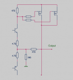
lineup said:.
I remove the source resistors in mosfets. This will increase the gain a bit. We may need source resistors, to control MOSFET current but let's try WITHOUT, to begin with.
Agreed. i think i said that in an earlyer post. The laterals have low gm and consequently rather low gain into theintended output load, so we want to maximize it.
I also agree with the redrawn CFP with gain as an experiment. i mentioned in my last post there are two basic ways to connect a CFP with gain, this is the other of the two. Assuming Q24, 34, 35 on the same heatsink, this should thermally compensate the BJTs, and we can, for now, leave the laterals to self-compensate, as they usually do.
One important thing when comparing to the Giesbert amp from Elektor - he also uses this configuration even though the vertical MOSFETs he uses, are not by any means self-compensating. But, he does put them on the same heatsink as the CFP BJTs so he gets compensation in this way. I should mention, however, that it is possible that giesberts amp would become thermally undercompensated over some value of bias current, although i think it is well otside any sane value one would want to use. This is a complex matter and i won't go into it here.
Now do we need a gain as much as 2, in this stage?
The answer is NO.
It may do very well with only 1.3-1.5.
If we could get any required drive voltage from the driver stage (within it's power rails, of course), I would agree, but we can't. For 60V power supply, the minimum CFP gain we want is that which is capable of producing 14V Vgs at clipped output, which means 60V-14V at the emitter of the BJTs. This gives us a minimum gain of 60/46 = 1.3.
however, the input stage topology is such that the maximum voltage swing you can get is equal to ONE of it's supply rails minus input voltage, and that is at saturation of the differential pair.
Why? Simple - the output is the mean of the two followers, upper and lower. The emitter of the follower can reach ~Vbe less than the supply rail if no current flows through the collector of the differential feeding it. If maximum current flows, 1/2 of tail, then we have to chose Rc so that it's voltage drop is equal tot he supply rail, i.e. collector of differential is at zero. Of course, this implies zero volts at input and means saturation of the differential transistor, at which point the emitter of the follower is at ~ -Vbe. This is as far as you can go - one full rail voltage, and that's assuming very high gain. If there is cascoding, the cascode reference voltage is subtracted from this. it also follows that the collector resistance of the differential must be chosen such that it produces exactly (Vrail - Vcascode)/2 at differential current balance - at least this makes the static calculation very simple
but because you get the output of the differential referenced to the voltage rail, and not ground, the input rails must be VERy well regulated and decoupled, PSRR is only 6dB!With 50V rails for the input, no cascoding and 1.3 gain of the output stage, it means 1.3 x 50Vpp = 65Vpp out of the possible 120Vpp - rather bad. So, we need a gain a bit higher than 2, about 2.4, perhaps as high as 2.6, no more (no need to make it saturate too much on clipping). Either that, or a higher supply voltage for the input stage.
- Status
- This old topic is closed. If you want to reopen this topic, contact a moderator using the "Report Post" button.
- Home
- Amplifiers
- Solid State
- AMP with inverting output stage mosfet