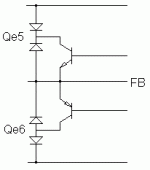
Both the schematic and the board itself is wired this way. Qe5~Qe8 are the current foldback, and although Qe6 and Qe8 look OK, Qe5 indeed has the emitter and collector reversed on the board as well as on the schematic.
So tell me I'm not nuts...Qe5 isn't ever going to work as intended unless it is reversed...right?
So tell me I'm not nuts...Qe5 isn't ever going to work as intended unless it is reversed...right?
An externally hosted image should be here but it was not working when we last tested it.
Hi,
Q5 looks wrong. But I wonder why it's there? Q7 & Q8 will work on their own without the darlington assist.
The protection locus omits the V part of IV and is not particularly good. I cannot assess the transient pass ability of the protection but it seems more comprehensive than usually seen.
I hate the way the schematic is drawn. that ground at the bottom is very confusing and worse it mixes power and signal together!
Usually there is a diode in series with the collectors of the VI-limiter. Maybe they were trying to achieve something similar. Q5 looks definitely wrong but I guess it actually works. It seems like the output transistors are not included in the schematic since they're not located on the board.
Originally posted by EchoWars
Both the schematic and the board itself is wired this way. Qe5~Qe8 are the current foldback, and although Qe6 and Qe8 look OK, Qe5 indeed has the emitter and collector reversed on the board as well as on the schematic.
So tell me I'm not nuts...Qe5 isn't ever going to work as intended unless it is reversed...right?
The circuit is a bit unusual... but work! In a direct mode Qe7 and Qe8 operate as a normal current limiter with Qe5 and Qe6 acting as collector diodes for Qe7 and Qe8.
In *REVERSE* mode (as may occur with some inductive load) Qe5 and Qe6 acts as clampers, so protecting the bases of output stages from voltage spikes originated by an inductive loal or by a sudden misconnecting of cable output (which often generate extravoltage spikes high enough to kill off the bases of output devices - singles or darlington, it's no a matter).
Hi
Piercarlo
darkfenriz said:but how about Q3 ?
Q3 in conjunction with Q4 form a normal darlington VAS Stage.
The base of Q3 connects to the LTP load resistor, the emitter connects to base of Q4 and to the negative rail via R13 (1K) and finally the colector connects to ground...
Hi,
Qe6 & Qe8 operate as a gain enhanced switch when triggered.
They obey all normal rules for orientation.
Why should Qe5 & Qe7 need to be orientated to break the normal rules?
I don't think the omission of the reverse voltage protection diodes affects the circuit operation.
I do think the diodes should be in there though, an omission that could lead to failure of the protection devices and then no protection.
But, can anyone explain why Qe6 & Qe8 need to be cascaded when Qe8 alone in saturation mode can source the current from the VAS?
AndrewT said:Hi,
Qe6 & Qe8 operate as a gain enhanced switch when triggered.
They obey all normal rules for orientation.
Why should Qe5 & Qe7 need to be orientated to break the normal rules?
(...)
But, can anyone explain why Qe6 & Qe8 need to be cascaded when Qe8 alone in saturation mode can source the current from the VAS?
One of two Q' (Qe5 or Qe6) is inverted. Which of two... BHO???
In my opinion is Qe6 inverted, not Qe5. In this circuit that is need is not further current amplification due to "transistor action" but just a couple of diodes which act just as diode in proper circumstances. Why the designer has not employed just a couple of diodes? Again: bho??? Pheraps for diminishing count part in manufacturing or avoid mounting mistakes (the system work equally with Qe5 and Qe6 reversed in emitter collector connections). However... is not a too "clean" job to do...
Hi
Piercarlo
If this makes the rest of the amp any easier to look at, here's the whole amp section redrawn. In this drawing, Q5 is oriented as one would expect, and the current foldback is not quite as shown in the first drawing, but what I'm interested in is if Q5 can possibly work with the emitter tied to the output line, and the collector tied to the base of the pre-driver...
Attachments
Q6 and Q8 look like they are wrong way around... Shouldn't emitter of a PNP connect feedback loop and collector (through a diode) the driver's base? Attached is a schematic showing part of the VI-limiter that was in the first schematic. I substituted transistors Q5 and Q6 with their "diode equivalents", should answer your question. A perfect reading concerning this matter is US patent 7,061,740 B2 by Eric Mendenhall.
Attachments
Tube_Dude said:
Q3 in conjunction with Q4 form a normal darlington VAS Stage.
The base of Q3 connects to the LTP load resistor, the emitter connects to base of Q4 and to the negative rail via R13 (1K) and finally the colector connects to ground...
You're right, I overlooked the fact that ground is on the botton of picture.
- Status
- This old topic is closed. If you want to reopen this topic, contact a moderator using the "Report Post" button.
- Home
- Amplifiers
- Solid State
- Isn't this like...wrong?