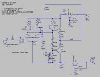
thought some here might find this interesting, has a lot of similarity to a power amp design. original design came from the Apt-Holman preamp, except that the Holman had a fet and a bipolar in the diff amp, but that causes a lot of offset, so i replaced the bipolar with another jfet. also replaced the RIAA network with just a resistor in the feedback loop.
-3db points are 2.5hz and 35khz
distortion: -60db (as-is with no tweaking) mostly even harmonic.
-3db points are 2.5hz and 35khz
distortion: -60db (as-is with no tweaking) mostly even harmonic.
Attachments
unclejed613:
Nice design, simple to understand.
A few questions:
- Did you just simulate it or have you actually built one?
- Temperature stability? PSRR? Output impedance?
- Why do you think one should/would use a discrete op-amp vs a modern audio opamp (2604, etc)?
Very interesting posting, hope you cna show us a picture soon of the working prototype.
AndrewT:
Can you explain your suggested changes/questions?
Hi Giga,
moving C3 takes out the Miller compensation and gives NFB over two stages rather than one. The Miller comp cripples the LTP.
I think the rather narrow 35kHz bandwidth is due to the gain being set to near +60db. I suspect that this discrete will never be used like a true opamp and it would be fairer to set the gain (and see the CL BW) to nearer where it will be in practice.
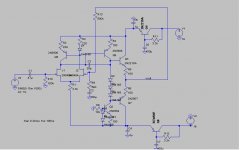
tnx...... it's what i get for working late hours..... q5 and q7 are backwards............. i'll redo it and rerun it.....
actually the circuit in it's original form (with a 2n3904 in place of j2) was a very successful phono preamp in the Apt-Holman preamp
tnx for the heads up out there...... unfortunately sims rarely tell you that you just let the "magic smoke" out of components..... those 2 backwards pnp's definitely would have given a nice smoke and light show.......
hi
it is a very simple op-amp circuit
very much standard,
except for
1. the JFET input
2. current mirror 'on top'
3. noise reduction transistors in supply rails
All these 3 features will probably add to improve this amplifier.
We can still get fantastic good performance from these kind of amps.
") Often much more performance than we ever need.
Often much more performance than we ever need.
At least if the load is not extremely 'heavy' (=very low resistance)
Nice circuit, unclejed
Regards
lineup
it is a very simple op-amp circuit
very much standard,
except for
1. the JFET input
2. current mirror 'on top'
3. noise reduction transistors in supply rails
All these 3 features will probably add to improve this amplifier.
We can still get fantastic good performance from these kind of amps.
Often much more performance than we ever need.At least if the load is not extremely 'heavy' (=very low resistance)
Nice circuit, unclejed
Regards
lineup
ok, here it is, corrected..... simmed it, and even harmonic distortion is gone, if you change the 25pf cap to 5pf, high freq -3db point is 90khz.....
ok, i guess i figured out how to tell when one has done something stupid in a sim..... if you make a fatal mistake (backwards transistor, applying negative feedback to an inverting input (i.e. a "double negative) or positive feedback to a noninverting input, etc...), the sim either takes a long time to find a dc operating point solution, or never finds one......
just like the rules for building a physical prototype, the rules for "sim building" should contain the following:
if you can't figure out why it's not working quite right, and you can't remember a> where you put the solder, or b> what transistor you were supposed to flip before adding resistors, you need some rest......
i'll be protoyping this after i get my parts unpacked.....
and to answer another question..... yes, but off the top of my head i can only remember.. the japanese equivalent of a 2n3904 would be a 2sc1318, and the 2n3906 would be a 2sa945, for the others, the "output devices" are 60v/800ma devices, and the jfets are 80v low noise jfets
the original gain of this when it was used as a phono preamp was about the same, but it's frequency response was an RIAA curve.....
now that i know what i did wrong, i'll try the combo (fet/bjt) diff amp again and see what, if any advantage there was in using it.
as far as the transistor power filters go, the published noise specs of this as a phono preamp are : 74db below 5mv (about -100dbV).
Attachments
unclejed613 said:
the original gain of this when it was used as a phono preamp was about the same, but it's frequency response was an RIAA curve.....
--------------
as far as the transistor power filters go, the published noise specs of this as a phono preamp are : 74db below 5mv (about -100dbV).
This was what I figured, when seeing those noise filters transistors.
That it was originally a RIAA phono amplifier.
Because of the very large gain (x1.000) such filters are sometimes used,
to avoid that noise from supply is also amplified 1.000 times.
What other amplifiers use high gain?
Yes, we can use it for microphone pre-amplifier.
The input from a microphone capsule, is typically a few mV.
Sometimes even below 1.0 mV.
1000 x 1 mV = 1 Volt, which is about at line level.
And so this level can be suitable for amplifiers' input.
lineup
all that needs to be done to reduce the gain is to change the ratio between R13 and R9......
i'm thinking that if the filters are removed, and R13 were replaced with a pot, this would make a great headphone amp as-is.
what interested me was it's similarity to a power amp...... it could be scaled up, replace the resistor in the diff amp with a current source, use a current mirror-current mirror to drive the VAS symmetrically, change the diode stack for a bias transistor, bigger output devices, higher voltage rails, etc......
i did sim it with a 2n3904 in place of j2. it lowers the distortion a little, but the offset is several volts at the output, even though there is a dc correction cap (C2) at the inverting input...... i think it has to do with the difference between the 0.7v bias required for the bjt, and the negative 1.5v required to bias the fet in the linear region.
btw, i was wrong about the pnp japanese transistor..... 2sa970, not 945
can of course be used with any lower gain
a headphone amplifier would not often need more gain than 4
sometimes only x1 = unity gain
======================================
The idea of using a input pair of transistors
is that they should be as perfectly alike (matched) as possibly can be.
Otherwise you get no good results, and of course an offset.
If you change the input pair, you should change both J1 and J2
to same type, and in reality these 2 transistor exemplars
should not only be BOTH 2N3904, but also
should be chosen to have as same data as possible:
- same Volt BE is the most important
- good if they have same hFE gain
======================================
Offset.
Try replacing D1 with a transistor, one 2N3906,
to match Volt-BE of Q5
... this replacement transistor (for D1) should be used like a diode
You attach Collector to Base
and the drop across this 'diode' will be = Base-Emitter
This may correct offset.
If you still do not get output offset around 0 Volt,
change the value of R4 ( 100 Ohm ), step by step,
until you get lowest possible offset.
====================================
For lower gains you could try removing C2,
as there is almost no base-current into a JFET, causing any offset-drop across resistors.
(unless maybe they are as big as R13, 500k)
Try for example R13 =47k, R9=15k and remove C2.
Instead connect R9 directly to Ground.
this will give a gain of:
(47/15) + 1, which is like ~ 4
When you lower gain, you may get instability.
If so, you should increase C3 (5pF) a bit .. maybe to 22/47pF,
until it is stable.
lineup
Hi
In the last amp I made, I observed the relationship to the amount of compensation (C3) needed for stability and the closed loop gain. Do you think this will be a factor here? If the pot(R13)
had a value of zero Ohms, would the amp be stable? The Av(voltage gain) should be constant. The volume pot should be on V3, as a voltage divider with the tap to C1.
Since the source/emitter voltage is +1.5V, then the proper place to bias the base of 2n3904 is +2.1V, not exactly zero. Also the jfets should be matched, at least Vgs at Id, for using real actual devices, or use a jfet pair IC.
R10 should be close to R9 in value, can cause stability issues with the input impeadance being so high and the input capacitance of J1, even though there is no gate current.......at DC(0Hz), higher frequency AC is another story.
You listed some improvements to change this circuit, replacing R1 with a CCS would be an improvement because the impeadance of it is very high above it's constant current giving better common mode rejection. Cascode is good too for input stage linearity, but risk of getting into the relm of the complex.

Hi Lineup
It appears to me if C2 were to be removed, then J1 & J2 must be matched perfectly or the DC offset will be the difference of J1_Vgs and J2_Vgs times Av. This would probably work for a duel jfet IC with a reasonable DC offset because they are identical. In my circuit with jfet diff input, I did notice an improvement to DC offset using the DC blocking cap, and also stability with AC signals. If the jfet legs conduct different currents during AC operation, wouldn't Vgs @ Id will be different as well? I suppose every circuit has it's unique properties though.
all that needs to be done to reduce the gain is to change the ratio between R13 and R9......
i'm thinking that if the filters are removed, and R13 were replaced with a pot, this would make a great headphone amp as-is.
In the last amp I made, I observed the relationship to the amount of compensation (C3) needed for stability and the closed loop gain. Do you think this will be a factor here? If the pot(R13)
had a value of zero Ohms, would the amp be stable? The Av(voltage gain) should be constant. The volume pot should be on V3, as a voltage divider with the tap to C1.
i did sim it with a 2n3904 in place of j2. it lowers the distortion a little, but the offset is several volts at the output, even though there is a dc correction cap (C2) at the inverting input...... i think it has to do with the difference between the 0.7v bias required for the bjt, and the negative 1.5v required to bias the fet in the linear region.
[/B]
Since the source/emitter voltage is +1.5V, then the proper place to bias the base of 2n3904 is +2.1V, not exactly zero. Also the jfets should be matched, at least Vgs at Id, for using real actual devices, or use a jfet pair IC.
R10 should be close to R9 in value, can cause stability issues with the input impeadance being so high and the input capacitance of J1, even though there is no gate current.......at DC(0Hz), higher frequency AC is another story.
You listed some improvements to change this circuit, replacing R1 with a CCS would be an improvement because the impeadance of it is very high above it's constant current giving better common mode rejection. Cascode is good too for input stage linearity, but risk of getting into the relm of the complex.
Hi Lineup
It appears to me if C2 were to be removed, then J1 & J2 must be matched perfectly or the DC offset will be the difference of J1_Vgs and J2_Vgs times Av. This would probably work for a duel jfet IC with a reasonable DC offset because they are identical. In my circuit with jfet diff input, I did notice an improvement to DC offset using the DC blocking cap, and also stability with AC signals. If the jfet legs conduct different currents during AC operation, wouldn't Vgs @ Id will be different as well? I suppose every circuit has it's unique properties though.
i found out why tom holman used the jfet-npn diff amp, even though it caused offset. it was to reduce noise.
i removed c3. -3db point moves up to 200khz, GBW becomes 70 Mhz, with the phase shift reaching 180 degrees at 35Mhz, while the gain is still 12db. without c3, this amp is not stable at gains of 12db or less, so it definitely cannot be used at a gain of 4, or unity gain without oscillating.
with 5pf compensation, the amp is stable to unity gain, GBW is 46Mhz, -3db point is at 94Khz.
with 2n3904's as the diff pair, the GBW is 66Mhz, and 180 degree phase shift at 36 Mhz, while the gain is 10db, which puts the amp back in unstable territory again. this is probably because of the junction capacitances of the NPN transistors. using NPN transistors bumps up the distortion about 10db. this is still with 5pf compensation
this amp seems like a good model to play with.... i think i'll test the jfet diff amp on other designs, especially one of the ones i've been working on that has instability problems.
i also played with different bias levels on the output transistors, and found that less bias causes more distortion.
1. It not good to have a gain potentiometer in the feedback
volume is to be used outside the amplifier.
Most have it in front of amplifier, but can be at amplifier output, too.
2. For JFET there is often not needed with the CAP C2 to ground.
C2 is for blocking DC-current.
BJT has got bias current into Base, some uA
JFET has almost no DC-current. Some 1000 times less maybe.
3. As I told, at lower gains, or unity gain
if C3 is omitted or too low, you can get instability
In a pure resistor load, it may show no instability.
But test for some capacitive load.
In reality, Typically we can count a connection wire or cable from preamp output
having anything from 10pF to some nF capacitance.
I used capacitance from 0 - 22nF to simulate one preamp today.
It had first upper -3dB bandwidth ~ 650.000 Hertz.
It was stable with 10nF but not in 22nF.
After some input RC lowpass filter and some compensation cap ( your C3 )
I got it stable in 1 kHz square wave and 22nF.
When testing bandwidth again, it was -3dB at just above 400.000 Hertz.
The gain of this preamp is x100.
Capacitance is put in parallel with load resistor.
Across the load.
A good start is 470pF / 1 nF, and run 1 kHz sinus and then square wave, at very low input level.
Use an oscilloscope to try to get good looking squarewave
I used 1 mV RMS in and 100 mV out.
The load I used and tested for was 22 kOhm.
lineup
Hi,
Then run through some different gains.
A phase margin of about 45degrees, closed loop, will give a little bit of peaking on a square wave test signal into a resistive load.
As the resistive load is paralleled with an increasing amount of load capacitance the phase margin drops until full oscillation is evident, but before this the tiny bit of peaking has become an increasing amount of damped ripple.
It is this damped ripple that some comentators attribute to increased/better treble when they change cables. NOT GOOD.
I think you should be looking for a good square wave into a variety of cap loadings at an acceptable gain. This may come when the phase margin is nearer 60degrees. It will also be easier to achieve with a small resistor on the output to isolate the load capacitance.
What happens if you reduce R5, R6 below 100r?
instead of removing C3, try moving it to the inverting base/gate.i removed c3. -3db point moves up to 200khz, GBW becomes 70 Mhz, with the phase shift reaching 180 degrees at 35Mhz, while the gain is still 12db. without c3, this amp is not stable at gains of 12db or less, so it definitely cannot be used at a gain of 4, or unity gain without oscillating.
Then run through some different gains.
A phase margin of about 45degrees, closed loop, will give a little bit of peaking on a square wave test signal into a resistive load.
As the resistive load is paralleled with an increasing amount of load capacitance the phase margin drops until full oscillation is evident, but before this the tiny bit of peaking has become an increasing amount of damped ripple.
It is this damped ripple that some comentators attribute to increased/better treble when they change cables. NOT GOOD.
I think you should be looking for a good square wave into a variety of cap loadings at an acceptable gain. This may come when the phase margin is nearer 60degrees. It will also be easier to achieve with a small resistor on the output to isolate the load capacitance.
What happens if you reduce R5, R6 below 100r?
- Status
- This old topic is closed. If you want to reopen this topic, contact a moderator using the "Report Post" button.
- Home
- Amplifiers
- Solid State
- discrete op amp