Hi,
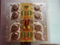
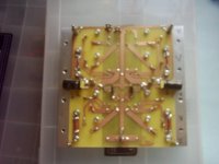
I have made a new board (or boards) for the superleach. Everything enclosed in red box in the schematic is on an output board which sits under the main as in the photos. I have solder all the to-3 onto the output board. Further I do not have a scope for what Mr. Leach is doing. Is there a way to test the main board by just using DVM and not desoldering the to-3's out? I only had one piece of board made.. If that is OK, I intend to send it to the fab-house. This prototype is going to be dismentaled after the testing.
Tks for the tip
BTW if I am really sending it to the fab house, I need to order 10 sets. I have plans for 4 sets, would anybody be interest in sharing the rest? They should be around US$35/set, 1.6mm FR4, component silkscreen, tinned 3oz copper with solder mask in blue.
Attachments
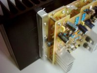
Andrew, you were right about that, tks. I forget to include them in the 'red box'. But they were there. If you re-examine the first photo (where you can see the heatsink) you can see a ele. cap. sandwiched between the 2 boards or should I say, soldered to the soldering side of output board. The one in between the middle 2 screws holding the alu. bar to the heatsink.
So any more tip for the testing?
So any more tip for the testing?
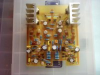
I also solder the 100nf along side with the 100uf or exactly 47uf as stated in Mr. Leach part list and hopefully that's not going to affect anything. Hope the attached photo can clarify that. Also I don't have MJE15030, 031 at hand so I use MJE15031, 032. Guess that should be OK too. The rest of the components I use exactly the same thing. The 11k and 1k1 I made it up with 22k nad 2k2 in parallel. The 6k2 was made up by serialing 3k and 3k3 to get as close as possible. You might see the mess of it on the main board. But I had modified the board for the fabrication version so that it can accomodate both parallel and serial resistors for the 6k2.
Attachments
that is a good suggestion that allows a lot of alternate component selection/experimenationmaking it EBCE
I would add multiple pin pitch pads to ALL capacitors.
AND leave room for a few polypropylene pitch caps in selected locations.
Ceramics can always be added on the back of the PCB directly to the legs of other components (if you have not snipped them already).
Add space/traces/pads for alternative stability components.
Add pin locations for test points.
Add second Vrail inputs for regulated Vrails to voltage amp.
testing boards without output devices
at APT, we did our amp board test with 1.5k/5w resistors across the output transistor b-e conections to test the drivers and bias circuit and board functionality. we had a bed-of-nails fixture for this, as well as plug-in (to-3 transistors with the transistor replaced by the 1.5k resistor) devices for troubleshooting after amps were assembled.
at APT, we did our amp board test with 1.5k/5w resistors across the output transistor b-e conections to test the drivers and bias circuit and board functionality. we had a bed-of-nails fixture for this, as well as plug-in (to-3 transistors with the transistor replaced by the 1.5k resistor) devices for troubleshooting after amps were assembled.
Hi,
just a thought and I might be far off base.
The DC voltages around the circuit are fixed when the amp is not oscillating.
You may find that what should be nice stable DC voltages move around to unpredictable values depending on what you have hanging on the output and/or input (or touch when probing around). The AC currents induced by ocscillation change the apparent DC voltages, but where to check as likely indicators, I don't know.
I cannot say that Leach amplifier need this accessorie during testings
But i am sure that many amplifiers have deserved a shot.
I gave some shots in amplifiers during this life...i am happy because of that.
This test accessorie is needed sometimes.
regards,
Carlos
But i am sure that many amplifiers have deserved a shot.
I gave some shots in amplifiers during this life...i am happy because of that.
This test accessorie is needed sometimes.
regards,
Carlos
Attachments

- Status
- This old topic is closed. If you want to reopen this topic, contact a moderator using the "Report Post" button.
- Home
- Amplifiers
- Solid State
- testing super leach without a scope