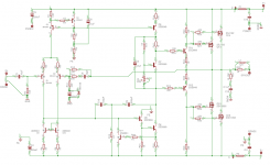
I was thinking of building the "Figure 11.6" amp from Randy Slone's "High Power Audio Amp Construction Manual". It's an L-MOSFET version of his "Figure 11.4" amp, which itself is an improved version of Self's Blameless.
I took the "Figure 11.6" schematic and made some changes. I removed the OPS current limiting circuit, and also removed the drain resistors from the OPS circuit. I've attached the resultant schematic. Will it work?
Removing the OPS resistors of course removes a convenient way to set the quiescent current. I had to remove the resistors purely because I didn't know how to fit the circuit into a 3.2"x4" Eagle PCB otherwise. If I didn't have space constraints, I'd have retained the resistors (and probably also the OPS current limiting).
I'm told that if there's no need to sense output current using the OPS resistors, then L-MOSFET OPS can work without output resistors. I based my circuit modifications on this.
Now that I don't have those resistors, I was thinking of using an experienced friend's lovely suggestion and use the rail fuse holder and an ammeter to set the quiescent current.
What do you think? Will it work?
Attachments
In order to produce a truly stable bias current, you would need to connect the driver emitters and corresponding LMOS drains together, and use small valued emitter resistors (similar to what was previously used for current sensing). With LMOS however this is not as big a concern as it would have been with a different type of MOSFET or a BJT, you might get awat with it.
Secondly, BJT-MOS CFPs are usually asking for trouble") but again, the low gm of the LMOS may help you there. It won't however help you with output swing, at full output current, you will have a 14V rail loss!
but again, the low gm of the LMOS may help you there. It won't however help you with output swing, at full output current, you will have a 14V rail loss!
Secondly, BJT-MOS CFPs are usually asking for trouble
but again, the low gm of the LMOS may help you there. It won't however help you with output swing, at full output current, you will have a 14V rail loss!So basically you are saying that it's not a crazy idea... one can try it. Great.ilimzn said:In order to produce a truly stable bias current, you would need to connect the driver emitters and corresponding LMOS drains together, and use small valued emitter resistors (similar to what was previously used for current sensing). With LMOS however this is not as big a concern as it would have been with a different type of MOSFET or a BJT, you might get awat with it.
You're right about the rail loss... 7V per device. I guess this also translates to increased heat dissipation. But then for domestic use, I guess it'll be used at moderate power levels most of the time, so I may never hit rail voltages other than for brief peaks.Secondly, BJT-MOS CFPs are usually asking for trouble
I don't understand almost anything about amplifier design, but I did notice that Randy has used a unity-gain 100% local feedback CFP OPS in the BJT version of this amp, and has added local gain in the OPS when he designed the MOSFET version (i.e. the one I've drawn). I believe this gain is being implemented by adding those resistors in the driver transistors' collector and emitter. I wonder why Randy made this change. Is this anything to do with the lower gm of the MOSFET devices as you mentioned?
Hi,
the ratio of r17 to r33 seems low.
How about adding 200r in series with r33 and dropping r33 to 1k0?
Use of 2sd669 for Q5 seems a bit odd. Consider a low Cob transistor here.
R22 might be a bit high. Starts to limit at 12mA.
Matching the output FETs will help, but re-inserting source resistors and matching would be better.
Have you considered using different value gate resistors for the P & Nchannel FETs?
I dislike the two CCSs fed from one control. Self never solved the asymetric slew.
Will the front end control the output offset if it runs off a supply that bypasses the fuses? i.e. fuse just the drivers and FETs.
No RF filter at the front end.
C7 seems a bit small.
BUT the big question!!!
Will the CFP work with these relatively fast transistors?
Where do you build in extra resource to debug and stabilise the output?
Ouch... you got me there. I'd made a change there without realising its impact. Randy had put something like an 800E for the R17, and had put a 220E in series with the R33, IIRC. I had thought my change wouldn't make a difference.AndrewT said:the ratio of r17 to r33 seems low.
How about adding 200r in series with r33 and dropping r33 to 1k0?
Use of 2sd669 for Q5 seems a bit odd. Consider a low Cob transistor here.
What's a low-Cob transistor?
I wish I could understand how the values of these resistors in the VAS are set.R22 might be a bit high. Starts to limit at 12mA.
Okay. But will it work reliably without source resistors?Matching the output FETs will help, but re-inserting source resistors and matching would be better.
I have not considered anything... I don't know enough about amp design to do so. But now that you mention it, I believe others have also said that one of the devices ideally needs larger gate resistors than the other. I forget which. I believe the 2SK1058 needs the higher gate resistor, IIRC.Have you considered using different value gate resistors for the P & Nchannel FETs?
How does asymmetric slew affect the sound? I know it will look asymmetric on the 'scope, but I don't know anything more.I dislike the two CCSs fed from one control. Self never solved the asymetric slew.
I didn't understand the question? What will I gain if I move the fuses to the "left" and leave the OPS unprotected?Will the front end control the output offset if it runs off a supply that bypasses the fuses? i.e. fuse just the drivers and FETs.
True. I guess I can think of adding something there if board real estate permits. I hate the Eagle size limit, and paying only takes it to 6"x4". I wish Eagle had the Vutrax limit on pin count, not board size.No RF filter at the front end.
What value do you suggest I should increase it to?C7 seems a bit small.
I don't think I know enough to even answer this question, but I believe Randy's tried this CFP with these devices, and it works fine, but he used OPS resistors, and I don't know what impact those resistors have on stability.BUT the big question!!!
Will the CFP work with these relatively fast transistors?
Where do you build in extra resource to debug and stabilise the output?
I believe you are referring to R23 to R26, and you are saying that R24 should not be there.... there should be a direct short between the MOSFET drain and the driver's emitter. But this design does not have that.ilimzn said:In order to produce a truly stable bias current, you would need to connect the driver emitters and corresponding LMOS drains together, and use small valued emitter resistors (similar to what was previously used for current sensing).
From what I've understood (which is extremely little) that sort of direct shorting would mean eliminating the four resistors R23 to R26, and would give you unity gain CFP with 100% local feedback. However, this particular design has less local feedback and some gain, achieved through those resistors. Slone said so in his very brief explanation of this circuit. And I've just retained it as it is.
How does one calculate the values of these resistors? Slone does not give any explanations in his book for these values.AndrewT said:the ratio of r17 to r33 seems low.
How about adding 200r in series with r33 and dropping r33 to 1k0?
In his "Figure 11.4" BJT based design with almost identical topology, Slone uses 820E for the R17, then the trimpot of 1K in series with a 100E resistor.
In his "Figue 11.6" design which is just an adaptation of 11.4 for L-MOSFETs, he uses 1K for R17, and a 220E in series with a 1K trimpot. I had removed the 220E, thinking that any resistance in series with a rheostat can be obtained by just setting the rheostat to an appropriate point.
I'm really curious to know how does one calculate the appropriate values for these resistors/trimpots?
Hi,
do you really want us to answer all those questions?
If you need that much information, I suspect that you should be doing much more research on how amplifiers work before modifying another's design.
You need to understand the purpose of each component and it's effect on it's neighbours before you decide, for good reasons, to alter it.
Have you read Leach and ESP and Pass?
Yes, I really do.AndrewT said:do you really want us to answer all those questions?
I modified the design to the extent that my "research" as you call it, allowed me to. In fact, I still consider my modifications to be marginal.If you need that much information, I suspect that you should be doing much more research on how amplifiers work before modifying another's design.
Or you need to make modifications which your "research" tells you are marginal, and then ask veterans on the Net, and learn from them. This process too is part of my "research".You need to understand the purpose of each component and it's effect on it's neighbours before you decide, for good reasons, to alter it.
I've read ESP (Rod is one of the guys who says that drain resistors from his L-MOSFET OPS can be left out), and Slone's books. I haven't read Self, and I've skimmed through Leach.Have you read Leach and ESP and Pass?
Just so that we know what mods we are talking about, I have made only two mods:
- I've removed the OPS protection components
- I've removed the OPS drain resistors
I wish we were spending this energy discussing my questions instead of my reading.
Hi Tc,
this is a bit long, sorry to others, who may want to skip this (unless I have made a mistake and need correction)
Here goes.
Q7 is a Vbe multiplier.
The active part multiplies the current to maintain the voltages set by the upper and lower legs of the resistive ladder.
The lower leg resistors will ALWAYS match the Vbe of Q7, that's where the title comes from.
The 1k:2k defines the minimum voltage produced about [1+(1k/2k)]*0.65~=1V
Setting the pot to 100r sets near maximum voltage, 1+1k/0.1k*0.65=17.5V and the output stage has just overheated and wasted itself.
Q5,
Look up the datasheet for a 2sa649/d669 and compare it to 2sa1360/c3423, Cob 27pF to 2.5pF a factor of 11.
Current limiting of Q6.
r22 set to 47r allows about 0.6v/47r~=12mA of current when it has started to switch on the protection transistor (Q17). Q17 probably starts to switch on at about 500mV and will progressively distort the signal as it's Vbe voltage rises. It will be fully limiting before Vbe reaches 700mV. I think the R47 should be set to at least allow double the VAS CCS current through and preferably three times the current. Some designers go as high as 5 or 6 times as much to ensure the distortion of initial triggering does not become audible on difficult loads. If the VAS needs 47r of degeneration then splitting the resistor in two and monitoring the current in the lower leg of the pair will give a more flexible choice of trigger current.
Source resistors,
the FETs case temperature will depend on device dissipation and heatsink temperature.
Omitting the source resistors will result in poorer matching of bias currents at idle and of output currents when driving the load. The device carrying more bias current will run warmer and when asked to carry output will also take a higher proportion of that as well (if the Gm is similar to it's partners). This will take the device nearer to the SOAR and the hottest device is the one likely to fail first. Fortunately, Laterals are self compensating. I have a 4pair amp that has closely matched Vgs and accurately matched source resistors. I can easily measure the difference in bias currents between them on the good side (Nchannel). I have one Pchannel that has Vgs about 30mV low and it draws nearly 30% more bias current than it's partners. It runs hot. A big THICK heatsink helps here.
Gate capacitance,
the Pchannel has significantly higher gate capacitance than the Nchannel. Putting equal value gate resistors in slows down (low pass filter) the Pchannel more than the Nchannel to changes in drive voltage. Many designers select a lower value gate resistor for the Pchannel to help speed it up a bit. Much debate on the proportional change required. Testing/development!
Slew & shared CCS,
Self spent about half a chapter showing how he failed to solve the asymetric slew that is endemic in his Miller compensated/common CCS circuit. I believe there is an advantage in using the shared CCS (something to do with recovery after clipping?), but Self never told us why he chose to use it, other than saving resources (poor reason). I would add the extra transistor and set my volume control to avoid clipping.
Output slew on fuse blowing.
I asked the wrong person, I don't have a solution.
But my description must have been ambiguous, my proposal was for the fuse in ONLY the driver/output rails. The voltage amp is unfused, not the other way wrong as you interpreted it. But I suspect this alone does not solve the problem.
RF filter,
just two small components. Add them or place them on the back of the input RCAs.
NFB high pass filter,
the RC is set to 220uF*330r=73mS. I think for a wideband amplifier this should be set to about 130 to 150mS, provided the PSU is set to 180 to 200mS. Setting C7 small saves money on smoothing capacitance (and attenuates the bass).
Sloan has shown a confusing variety of ground types. Take care not to common the wrong ones. You need at least two separate types of ground connection from the PCB. or, ALL your other grounds have to come to the PCB central ground (not particularly neat).
Go and read Leach and learn it till it comes out your ears. You may eventually disagree with some of his decisions but that simply means you have learned to recognise the shortcomings he has included in his various iterations.
this is a bit long, sorry to others, who may want to skip this (unless I have made a mistake and need correction)
If all you removed/changed were those two items then I think my other comments reflect on the competance of the designer. I don't think much of Sloan , if this is the standard of his work (unless someone else has changed component values). But there again, maybe he has built this design and optimised it to produce the goods, I'm only looking at it theoretically.the ratio of r17 to r33 seems low.
How about adding 200r in series with r33 and dropping r33 to 1k0?
Use of 2sd669 for Q5 seems a bit odd. Consider a low Cob transistor here.
R22 might be a bit high. Starts to limit at 12mA.
Matching the output FETs will help, but re-inserting source resistors and matching would be better.
Have you considered using different value gate resistors for the P & Nchannel FETs?
I dislike the two CCSs fed from one control. Self never solved the asymetric slew.
Will the front end control the output offset if it runs off a supply that bypasses the fuses? i.e. fuse just the drivers and FETs.
No RF filter at the front end.
C7 seems a bit small.
......Where do you build in extra resource to debug and stabilise the output?
Here goes.
Q7 is a Vbe multiplier.
The active part multiplies the current to maintain the voltages set by the upper and lower legs of the resistive ladder.
The lower leg resistors will ALWAYS match the Vbe of Q7, that's where the title comes from.
The 1k:2k defines the minimum voltage produced about [1+(1k/2k)]*0.65~=1V
Setting the pot to 100r sets near maximum voltage, 1+1k/0.1k*0.65=17.5V and the output stage has just overheated and wasted itself.
Q5,
Look up the datasheet for a 2sa649/d669 and compare it to 2sa1360/c3423, Cob 27pF to 2.5pF a factor of 11.
Current limiting of Q6.
r22 set to 47r allows about 0.6v/47r~=12mA of current when it has started to switch on the protection transistor (Q17). Q17 probably starts to switch on at about 500mV and will progressively distort the signal as it's Vbe voltage rises. It will be fully limiting before Vbe reaches 700mV. I think the R47 should be set to at least allow double the VAS CCS current through and preferably three times the current. Some designers go as high as 5 or 6 times as much to ensure the distortion of initial triggering does not become audible on difficult loads. If the VAS needs 47r of degeneration then splitting the resistor in two and monitoring the current in the lower leg of the pair will give a more flexible choice of trigger current.
Source resistors,
the FETs case temperature will depend on device dissipation and heatsink temperature.
Omitting the source resistors will result in poorer matching of bias currents at idle and of output currents when driving the load. The device carrying more bias current will run warmer and when asked to carry output will also take a higher proportion of that as well (if the Gm is similar to it's partners). This will take the device nearer to the SOAR and the hottest device is the one likely to fail first. Fortunately, Laterals are self compensating. I have a 4pair amp that has closely matched Vgs and accurately matched source resistors. I can easily measure the difference in bias currents between them on the good side (Nchannel). I have one Pchannel that has Vgs about 30mV low and it draws nearly 30% more bias current than it's partners. It runs hot. A big THICK heatsink helps here.
Gate capacitance,
the Pchannel has significantly higher gate capacitance than the Nchannel. Putting equal value gate resistors in slows down (low pass filter) the Pchannel more than the Nchannel to changes in drive voltage. Many designers select a lower value gate resistor for the Pchannel to help speed it up a bit. Much debate on the proportional change required. Testing/development!
Slew & shared CCS,
Self spent about half a chapter showing how he failed to solve the asymetric slew that is endemic in his Miller compensated/common CCS circuit. I believe there is an advantage in using the shared CCS (something to do with recovery after clipping?), but Self never told us why he chose to use it, other than saving resources (poor reason). I would add the extra transistor and set my volume control to avoid clipping.
Output slew on fuse blowing.
I asked the wrong person, I don't have a solution.
But my description must have been ambiguous, my proposal was for the fuse in ONLY the driver/output rails. The voltage amp is unfused, not the other way wrong as you interpreted it. But I suspect this alone does not solve the problem.
RF filter,
just two small components. Add them or place them on the back of the input RCAs.
NFB high pass filter,
the RC is set to 220uF*330r=73mS. I think for a wideband amplifier this should be set to about 130 to 150mS, provided the PSU is set to 180 to 200mS. Setting C7 small saves money on smoothing capacitance (and attenuates the bass).
Sloan has shown a confusing variety of ground types. Take care not to common the wrong ones. You need at least two separate types of ground connection from the PCB. or, ALL your other grounds have to come to the PCB central ground (not particularly neat).
Go and read Leach and learn it till it comes out your ears. You may eventually disagree with some of his decisions but that simply means you have learned to recognise the shortcomings he has included in his various iterations.
Hi Tcpip,
In your original post you said that you left the source resistors etc. out because of space constraints (presumably of the Eagle software). You shouldn't let details like that affect your designs.
If you didn't know, Protel's Autotrax is available as a free download. It's small (dos based), easy to use, allows you to create your own component libraries, and supports very large board sizes (about 36" by 36 " I think).
Here's a link:
http://www.altium.com/Community/Support/Downloads/
There's also a Windows XP video driver available at:
http://www.airborn.com.au/layout/easytrax.html
I hope this helps
AndrewT, thanks hugely for the patient reply.
How do you decide what CCS current you need for a VAS when doing a fresh design?
What if I remove the VAS current limiting (Q17 and R20) completely?
Am I right in saying that R14 sets the VAS CCS current in my circuit?
Other than that, I understood your current limiting discussion completely, I think.
Thanks for your huge patience. You've made a permanent difference to my knowledge about amp design.
I'm still trying to work my way through this. It'll take a bit of time. I thought I'd respond to the rest first.AndrewT said:Q7 is a Vbe multiplier.
The active part multiplies the current to maintain the voltages set by the upper and lower legs of the resistive ladder.
The lower leg resistors will ALWAYS match the Vbe of Q7, that's where the title comes from.
The 1k:2k defines the minimum voltage produced about [1+(1k/2k)]*0.65~=1V
Setting the pot to 100r sets near maximum voltage, 1+1k/0.1k*0.65=17.5V and the output stage has just overheated and wasted itself.
I know now what you meant. Is this important only for Q5? What about the drivers (Q11, Q12)?Q5,
Look up the datasheet for a 2sa649/d669 and compare it to 2sa1360/c3423, Cob 27pF to 2.5pF a factor of 11.
I understood what you described about the R22 setting the current limit... Slone's book describes this process while explaining CCS and OPS protection circuits. But I didn't know what a designer shoots for when deciding VAS current limits; Slone's book never mentioned it. Your description filled in that bit. Thanks a lot.Current limiting of Q6.
r22 set to 47r allows about 0.6v/47r~=12mA of current when it has started to switch on the protection transistor (Q17). Q17 probably starts to switch on at about 500mV and will progressively distort the signal as it's Vbe voltage rises. It will be fully limiting before Vbe reaches 700mV. I think the R47 should be set to at least allow double the VAS CCS current through and preferably three times the current. Some designers go as high as 5 or 6 times as much to ensure the distortion of initial triggering does not become audible on difficult loads. If the VAS needs 47r of degeneration then splitting the resistor in two and monitoring the current in the lower leg of the pair will give a more flexible choice of trigger current.
How do you decide what CCS current you need for a VAS when doing a fresh design?
What if I remove the VAS current limiting (Q17 and R20) completely?
Am I right in saying that R14 sets the VAS CCS current in my circuit?
Other than that, I understood your current limiting discussion completely, I think.
Got it. Basically, if I understand it correctly, my omitting the OPS resistors is not a good idea, but the amp may still work.Source resistors,
the FETs case temperature will depend on device dissipation and heatsink temperature.
Omitting the source resistors will result in poorer matching of bias currents at idle and of output currents when driving the load. The device carrying more bias current will run warmer and when asked to carry output will also take a higher proportion of that as well (if the Gm is similar to it's partners). This will take the device nearer to the SOAR and the hottest device is the one likely to fail first. Fortunately, Laterals are self compensating. I have a 4pair amp that has closely matched Vgs and accurately matched source resistors. I can easily measure the difference in bias currents between them on the good side (Nchannel). I have one Pchannel that has Vgs about 30mV low and it draws nearly 30% more bias current than it's partners. It runs hot. A big THICK heatsink helps here.
Yes, this part I understood completely. In fact, in Slone's second book, "Audiophile Projects Sourcebook", he has power amp schematics where he himself has switched to putting different values for gate resistors for MOSFET designs. I think Rod Elliott's P101 also uses different values (he uses gate resistors only on one half and not on the other, I think).Gate capacitance,
the Pchannel has significantly higher gate capacitance than the Nchannel. Putting equal value gate resistors in slows down (low pass filter) the Pchannel more than the Nchannel to changes in drive voltage. Many designers select a lower value gate resistor for the Pchannel to help speed it up a bit.
Basically, you're saying I should add another Q4 and R7 to the rear of Q8, right? Slone mentions the shared CCS purely as a transistor-saving technique.Slew & shared CCS,
Self spent about half a chapter showing how he failed to solve the asymetric slew that is endemic in his Miller compensated/common CCS circuit. I believe there is an advantage in using the shared CCS (something to do with recovery after clipping?), but Self never told us why he chose to use it, other than saving resources (poor reason). I would add the extra transistor and set my volume control to avoid clipping.
Initially I couldn't make head or tail of what you were saying here, but I think it's finally clicked. Basically you're saying that if one rail fuse blows and the other doesn't, then there'll be huge DC on the speaker output, right? I hadn't thought that far. If I don't put the fuse before the OPS, then I thought the purpose of the fuse is not served, is it? I thought the fuses were there to protect the OPS, no?Output slew on fuse blowing.
I asked the wrong person, I don't have a solution.
But my description must have been ambiguous, my proposal was for the fuse in ONLY the driver/output rails. The voltage amp is unfused, not the other way wrong as you interpreted it. But I suspect this alone does not solve the problem.
I understood this one. This is just a parallel pair of one C and one R, both connecting the signal input to the signal-ground, right?RF filter,
just two small components. Add them or place them on the back of the input RCAs.
This was one more area where I had no basis earlier for calculating the values of the components. I now know. I can always increase C7 to any value, maybe 1000uF.NFB high pass filter,
the RC is set to 220uF*330r=73mS. I think for a wideband amplifier this should be set to about 130 to 150mS, provided the PSU is set to 180 to 200mS. Setting C7 small saves money on smoothing capacitance (and attenuates the bass).
I was trying to design my PCB to have an external HQG and make the following ground links:Sloan has shown a confusing variety of ground types. Take care not to common the wrong ones. You need at least two separate types of ground connection from the PCB. or, ALL your other grounds have to come to the PCB central ground (not particularly neat).
- a signal ground which would connect the NFB ground and input signal ground to the HQG (called INGND)
- two grounds for the two sets of decoupling caps, close to the V+ and V- input points (called PGND1 and PGND2)
Does he have books, or are you just referring to his amplifier Web pages? I'll go look them up. I've never read his theoretical discussions carefully the way I've read some of Self and ESP and most of Slone.Go and read Leach and learn it till it comes out your ears.
Thanks for your huge patience. You've made a permanent difference to my knowledge about amp design.
Hi Tc,
It's the tiny available current from the LTP that must be designed for. The drivers have more current drive from the VAS, they also need good power and current ability of their own and cannot be made to survive with a low Cob.
VAS CCS current seems to vary between 3mA and 30mA depending on what follows, what the VAS itself can stand, what current best suits the VAS characteristics and the designer's choices.
Remove current limiting and you risk losing the VAS due to overcurrent, either due to a difficult load or due to output abuse.
R14 and the controlling Q4 set the VAS current.
Yes, it will still work, but how unbalanced are the case temperatures and for how long. Be gentle, it may run forever and sound OK.
Yes, copy the current setting CCS for both transistors. But keep in mind some do not agree with this view.
The fuses will NEVER be fast enough to protect the semiconductors. Some humous wag once said we put semis in to protect the fuses. He was so close to correct that it gets requoted often. The fuses will provide longterm protection to save the heatsinks melting and if correctly rated may save a bass driver from burning out.
Don't make c7 too big. Remember that correlation to PSU.
tcpip said:Is this important only for Q5? What about the drivers (Q11, Q12)?
..........How do you decide what CCS current you need for a VAS when doing a fresh design?
What if I remove the VAS current limiting (Q17 and R20) completely?
Am I right in saying that R14 sets the VAS CCS current in my circuit?
..............the amp may still work.
............I should add another Q4 and R7 to the rear of Q8, right?
.......I thought the fuses were there to protect the OPS, no?
..........I can always increase C7 to any value, maybe 1000uF.
...... his amplifier Web pages? I'll go look them up. I've never read his theoretical discussions carefully.............
It's the tiny available current from the LTP that must be designed for. The drivers have more current drive from the VAS, they also need good power and current ability of their own and cannot be made to survive with a low Cob.
VAS CCS current seems to vary between 3mA and 30mA depending on what follows, what the VAS itself can stand, what current best suits the VAS characteristics and the designer's choices.
Remove current limiting and you risk losing the VAS due to overcurrent, either due to a difficult load or due to output abuse.
R14 and the controlling Q4 set the VAS current.
Yes, it will still work, but how unbalanced are the case temperatures and for how long. Be gentle, it may run forever and sound OK.
Yes, copy the current setting CCS for both transistors. But keep in mind some do not agree with this view.
The fuses will NEVER be fast enough to protect the semiconductors. Some humous wag once said we put semis in to protect the fuses. He was so close to correct that it gets requoted often. The fuses will provide longterm protection to save the heatsinks melting and if correctly rated may save a bass driver from burning out.
Don't make c7 too big. Remember that correlation to PSU.
I have a problem not shared by many on this forum. I use Linux.kiwiandy said:In your original post you said that you left the source resistors etc. out because of space constraints (presumably of the Eagle software). You shouldn't let details like that affect your designs.
That's why Eagle and Vutrax are the only semi-professional or professional solutions I can easily use.
Of these, I find Eagle about a thousand times easier to use than Vutrax. I haven't been able to figure out Vutrax enough to even design the smallest PCB yet. Why, I can't even figure out what components the Vutrax library has.
Thanks for the suggestion anyway... if I ever switch to Windows for PCB design, I'll look up Protel.
Thanks again for the prompt and patient reply.
You haven't told me where to find Leach's writings, other than his Low-TIM amp Webpages.
You haven't told me where to find Leach's writings, other than his Low-TIM amp Webpages.
AndrewT said:Am I then right in believing that a Darlington VAS will hardly put any load on the input stage?VAS CCS current seems to vary between 3mA and 30mA depending on what follows, what the VAS itself can stand, what current best suits the VAS characteristics and the designer's choices.
Okay, I'll keep it. I may split the 47R resistor into two about-equal halves though, based on your suggestion.Remove current limiting and you risk losing the VAS due to overcurrent, either due to a difficult load or due to output abuse.
Good, then that part was correct.R14 and the controlling Q4 set the VAS current.
If I make two independent CCS, I don't have to change any values of any resistors, right? The current setting of the VAS CCS is already being set by the R14, and that will continue. I'll just add another transistor and a 1K base resistor whose value is non-critical for setting the CCS current. Am I right?Yes, copy the current setting CCS for both transistors. But keep in mind some do not agree with this view.
Oh... okay. I was under the impression that L-MOSFETs are so robust that fuses will often blow before the device is destroyed. For BJT OPS of course whatever that Mr Wag said applies.The fuses will NEVER be fast enough to protect the semiconductors.
Yes, this part I'm still trying to figure out. Why should the decoupling caps' time constant be longer than that of the NFB circuit? And how do you calculate the time constant of the decoupling caps? I mean, there's no R to calculate RC with, is there? Do you just calculate the current flow at full load and go with that?Don't make c7 too big. Remember that correlation to PSU.
Thanks again.
the capacitance of the transistor and added capacitance of the Miller comp load the LTP.tcpip said:.......Low-TIM amp Webpages.
Darlington VAS will hardly put any load on the input stage?
If I make two independent CCS, I don't have to change any values of any resistors, right? The current setting of the VAS CCS is already being set by the R14, and that will continue. I'll just add another transistor and a 1K base resistor whose value is non-critical for setting the CCS current. Am I right?
this part I'm still trying to figure out. Why should the decoupling caps' time constant be longer than that of the NFB circuit? And how do you calculate the time constant of the decoupling caps? I mean, there's no R to calculate RC with, is there? Do you just calculate the current flow at full load and go with that?
You don't need a base resistor for the CCS.
PSU time constant = speaker impedance * smoothing capacitance.
try +-20mF for 8ohm and +-40mF for 4ohm.
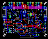
The PCB
I tried to design a PCB for this circuit, and this is what I got.
It has three power grounds and one signal ground, all meant to be separately connected to an off-board star ground. The signal ground just provides the ground reference for the input signal and the NFB components. All other grounds are connected to one of the other three ground points.
I've kept space for a Bourns 3299 trimpot; a slimmer 3296 will fit in the same space (I believe the 3299 is supposed to be more reliable, because it has multiple wipers, not just one).
Transistor pairs for CCS, LTP diff pair, and current mirror can be made to be close to each other.... it'll take me a few minutes of work.
You can see the board is fairly tightly packed in spite of being DS PTH, because of the small Eagle board size constraints.
Will this PCB work? This is my first power amp PCB attempt.
Attachments
Hi AndrewT,
Sorry I couldn't respond earlier, was away at some conferences all day, and today'll be some similar nonsense. But I've been reading Slone's book about the amplified-diode circuit, and trying to understand it. Your explanation makes it clearer than where I was after reading his book.
The small resistor in series with the rheostat is basically for safety, right? To prevent the builder setting too high a Vbias inadvertently?
One general question: will a one-size-fits-all 1K:1K voltage divider do for all situations? How do you decide what value of trimpot to use for a particular amp?
But I'm confused with respect to one fact: when reading Rod Elliott's P3A construction instructions, he says "start by setting the rheostat to the minimum resistance." If I've understood you right, this is dangerous because this is when the biasing will be maximum. (Rod's design uses a 1K:2K voltage divider, incidentally.) Did I understand Rod wrong, then? I've built a P3A pair.... does this mean I just got lucky when building it?
I looked at my amp PCB (posted in the previous post) and found that there's enough space to easily add one more resistor near the trimpot. I'll do that now.
Q7 is a Vbe multiplier.
The active part multiplies the current to maintain the voltages set by the upper and lower legs of the resistive ladder.
The lower leg resistors will ALWAYS match the Vbe of Q7, that's where the title comes from.
The 1k:2k defines the minimum voltage produced about [1+(1k/2k)]*0.65~=1V
Setting the pot to 100r sets near maximum voltage, 1+1k/0.1k*0.65=17.5V and the output stage has just overheated and wasted itself.
Sorry I couldn't respond earlier, was away at some conferences all day, and today'll be some similar nonsense. But I've been reading Slone's book about the amplified-diode circuit, and trying to understand it. Your explanation makes it clearer than where I was after reading his book.
The small resistor in series with the rheostat is basically for safety, right? To prevent the builder setting too high a Vbias inadvertently?
One general question: will a one-size-fits-all 1K:1K voltage divider do for all situations? How do you decide what value of trimpot to use for a particular amp?
But I'm confused with respect to one fact: when reading Rod Elliott's P3A construction instructions, he says "start by setting the rheostat to the minimum resistance." If I've understood you right, this is dangerous because this is when the biasing will be maximum. (Rod's design uses a 1K:2K voltage divider, incidentally.) Did I understand Rod wrong, then? I've built a P3A pair.... does this mean I just got lucky when building it?
I looked at my amp PCB (posted in the previous post) and found that there's enough space to easily add one more resistor near the trimpot. I'll do that now.
What is the correlation between the NFB HP time constant and the rail decoupling caps time constant?AndrewT said:NFB high pass filter,
the RC is set to 220uF*330r=73mS. I think for a wideband amplifier this should be set to about 130 to 150mS, provided the PSU is set to 180 to 200mS. Setting C7 small saves money on smoothing capacitance (and attenuates the bass).
And when calculating the PSU time constant, should I just take the on-board rail decoupling C into account, or also the off-board cap bank's C?
Thanks again.
Hi Tc,
correct. It also reduces the sensitivity of setting the pot at the low resistance end.tcpip said:The small resistor in series with the rheostat is basically for safety, right? To prevent the builder setting too high a Vbias inadvertently?
try to get the resistor current greater than ten times the base current, to minmise variations in transistor CE current modulating the ladder ratio by sucking current from the middle of the ladder.One general question: will a one-size-fits-all 1K:1K voltage divider do for all situations? How do you decide what value of trimpot to use for a particular amp?
maybe ESP had the pot on the collector side. You MUST put the pot+resistor between the base and emitter to avoid increase in current if the wiper goes momentarily or permanently open circuit. You set for minimum bias voltage which gives minimum bias voltage and this requires maximum resistance in the BE resistor leg. Neither should the base be connected to the wiper.reading Rod Elliott's P3A construction instructions, he says "start by setting the rheostat to the minimum resistance." If I've understood you right, this is dangerous because this is when the biasing will be maximum. (Rod's design uses a 1K:2K voltage divider, incidentally.) Did I understand Rod wrong, then?
as far as I know, none.
What is the correlation between the NFB HP time constant and the rail decoupling caps time constant?
nobody fits +-20mF to +-40mF as decoupling. Local decoupling is usually in the range 47uF to 220uF. It's a PSU calculation=smoothing capacitance.And when calculating the PSU time constant, should I just take the on-board rail decoupling C into account, or also the off-board cap bank's C?
- Status
- This old topic is closed. If you want to reopen this topic, contact a moderator using the "Report Post" button.
- Home
- Amplifiers
- Solid State
- Randy Slone "Fig 11.6" amp, modded: will work?