Hi,
the location of the fuses whether on the PCB or in the lines feeding the PCB or at the smoothing caps makes no difference to the level of protection offered to the downstream end.
The FETs must never see more than 15V across the gate source leads, otherwise they fail instantly.
Similarly if you look at the gate drain voltage (Vds) v drain current (Id) you see a limiting current for each Vgs.
If you select a suitable Vgs limit you can just about set a Current limit on the FET. It is this Vgs v Id that is the main short term protection for the FET. Continued current draw at this level then breaks the fuse.
Omit the Zener and the FET blows before the fuse.
You also need the Zener to catch any spikes that come into the gate.
tcpip said:
You mean I cut the negative rail between the bottom of R22 and the bottom of R26, and insert this resistor?
On this subject, I was wondering about the entire idea of doing additional decoupling of both rails between the OPS and the VAS. Is this a good idea? So few amps seem to do it.
If I imagine that the input power supply flows into the circuit near the OPS and then flows from right to left towards the VAS and then towards the input, then the maximum surges of current are in the OPS, and the VAS and input stages get the side-effects of this. Is it a good idea to cut each supply rail between the OPS and VAS, and put in an RC there?
Taking the idea one step forward, since the OPS will occasionally sink huge amounts of current, maybe there will be momentary current flow depletion for the VAS and input stages. So, to prevent this, maybe we could fit diodes (1N4001?) before the RC filters. That way, the supply current would flow in and charge the cap, but would never flow out.
What do you think? And if yes, then what values of RC make sense? We can estimate the current draw of the VAS and input stages by looking at the CCS resistors I guess.
I think that you are absolutely right in every aspect here. Choose rail resistor so that VAS and input stage do not "lose" too much volts. If your input stage and VAS consume 8mA or so, than with 330R in rail they will lose only 2.5V. If it is too much for you choose lower value.
Caps as big as possible
")
regards
Re: Managed to add OPS drain resistors
Power resistors on drains servo no purpose, waste of space on PCB in my opinion.
Andrew
I think, that 'ground' from output stage decoupling should go back to star point, maybe I don't understand your question...
tcpip said:
You can see the four power resistors. I've added one vertically (R34). This one will almost certainly have to be fitted on the underside of the PCB. (This of course implies that I'll need that much empty space below the PCB in my chassis.) The other three may either be fitted on the top surface, raised by a quarter inch, or on the bottom, as is found convenient. The inductor (marked "L1+R") will be fitted on top, raised by half an inch or even more above the PCB.
What do you think?
Power resistors on drains servo no purpose, waste of space on PCB in my opinion.
Andrew
I think, that 'ground' from output stage decoupling should go back to star point, maybe I don't understand your question...
Nice work. TCPIP
Is it by any chnce possible that you could uplod the schematics and Brd files for eagle CAD. I have two rails of BUZ lateral fets and this amp seems well suited to put them to Work
Thanx
www.eben.dk
Is it by any chnce possible that you could uplod the schematics and Brd files for eagle CAD. I have two rails of BUZ lateral fets and this amp seems well suited to put them to Work
Thanx
www.eben.dk
Re: Re: Managed to add OPS drain resistors
Hi Dark,
the bypass has to connect from the supply side of the active device to the ground side of the load to complete the circuit for "hi speed current".
The problem is that the distance between these two bypass connection points is very large.
The distance will increase the inductance in the connecting links and that inductance defeats the capacitance and the attenuating ability of the bypass.
It seems to me that the problem is not solved.
Is there another place to return the bypass that will "do the job" other than the ground side of the load?
Hi Dark,
Q.When output device bypasses are added, do they return to the ground side of the load?
What if the ground side of the load does not return to the PCB?
You understand perfectly.darkfenriz said:I think, that 'ground' from output stage decoupling should go back to star point, maybe I don't understand your question...
the bypass has to connect from the supply side of the active device to the ground side of the load to complete the circuit for "hi speed current".
The problem is that the distance between these two bypass connection points is very large.
The distance will increase the inductance in the connecting links and that inductance defeats the capacitance and the attenuating ability of the bypass.
It seems to me that the problem is not solved.
Is there another place to return the bypass that will "do the job" other than the ground side of the load?
Can I then just assume that R1 drops 0.6V and R14 drops another 0.6V, and use those to calculate the currents for the input and VAS respectively?darkfenriz said:I think that you are absolutely right in every aspect here. Choose rail resistor so that VAS and input stage do not "lose" too much volts. If your input stage and VAS consume 8mA or so, than with 330R in rail they will lose only 2.5V. If it is too much for you choose lower value.
Caps as big as possible
BTW, why does it matter even if the R that I add drops 2.5V? Don't these amps run happily with a fairly wide range of rail voltages (as in +/-10%)? This amp, as given in Slone's book, is rated for +/-55V supply. Should a drop of 2-3V matter?
Secondly, will it be effective without the resistor? What about just using a diode and caps?
I'll certainly pass it on, but please give it a few more days to stabilise it. I'm making changes almost every day now.MiiB said:Nice work. TCPIP
Is it by any chnce possible that you could uplod the schematics and Brd files for eagle CAD. I have two rails of BUZ lateral fets and this amp seems well suited to put them to Work
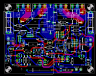
v5: with diodes and moved decoupling caps
I've managed to move the first set of decoupling caps (C11 and C12) close to the OPS, and there are additional decoupling caps (C3+C14, C4+C15) "after" the supply-rail diodes for the input and VAS. These are "near" the input section.
I'll now have to think of finding space for adding resistors "after" the supply-rail diodes.
The supply-rail diodes are marked as 1N4148 in the schematic. Please don't pay attention to that... I'll use 1N400x series devices. I just don't have appropriate packages in the Eagle library for 1N400x. And of course, cap values and resistor values are all up for discussion... they don't affect the PCB layout usually, so I'm going ahead with the layout. For instance, should C3 and C4 be 220uF or 1000uF, or something else?
I've managed to move the first set of decoupling caps (C11 and C12) close to the OPS, and there are additional decoupling caps (C3+C14, C4+C15) "after" the supply-rail diodes for the input and VAS. These are "near" the input section.
An externally hosted image should be here but it was not working when we last tested it.
An externally hosted image should be here but it was not working when we last tested it.
I'll now have to think of finding space for adding resistors "after" the supply-rail diodes.
The supply-rail diodes are marked as 1N4148 in the schematic. Please don't pay attention to that... I'll use 1N400x series devices. I just don't have appropriate packages in the Eagle library for 1N400x. And of course, cap values and resistor values are all up for discussion... they don't affect the PCB layout usually, so I'm going ahead with the layout. For instance, should C3 and C4 be 220uF or 1000uF, or something else?
There's loads of packages for diodes in the "diode" library, don't just look at the devices that specify a type.
There is a multiple package device in the "diode" library called "DIODE-" which has lots of packages. DO-27 size is probably most appropriate for flyback diodes.
There is a multiple package device in the "diode" library called "DIODE-" which has lots of packages. DO-27 size is probably most appropriate for flyback diodes.
Hi,
you don't need extra supply rail resistor to create an RC supply.
the diode/cap does that. The rail trace provides a little inductance and tiny resistance to create an LRC filter. If you do add a resistor (to listen for it's sound effect) then it can be before or after the diode or instead of the diode.
The small cap should catch the high frequency glitches and spikes and the big electro catches the low frequency modulations.
You may find that upto 1mF is useful and try to ease some space around (or move very slightly to optimise the space available) the present cap to allow different package sizes.
v7: added resistors
Added two resistors with the two diodes on the supply rails (see R38 and R39). Also added a resistor (R40) at the input, because without it, and with C2, there is a likelihood of oscillation (Q1 can become a common-base oscillator if its base finds an AC ground path, and C2 will provide that path if I don't add R40).
Now I'll have to increase the value of R10 slightly, so that it equals the sum of R4 and R40. Maybe I should make it 11K?
And best wishes for 2007, all you guys. I'm drinking some good, sweet, Sula Chenin Blanc "Late Harvest" as I write this.
Added two resistors with the two diodes on the supply rails (see R38 and R39). Also added a resistor (R40) at the input, because without it, and with C2, there is a likelihood of oscillation (Q1 can become a common-base oscillator if its base finds an AC ground path, and C2 will provide that path if I don't add R40).
An externally hosted image should be here but it was not working when we last tested it.
An externally hosted image should be here but it was not working when we last tested it.
Now I'll have to increase the value of R10 slightly, so that it equals the sum of R4 and R40. Maybe I should make it 11K?
And best wishes for 2007, all you guys.
I'm drinking some good, sweet, Sula Chenin Blanc "Late Harvest" as I write this. Yup, found it.jaycee said:There is a multiple package device in the "diode" library called "DIODE-" which has lots of packages. DO-27 size is probably most appropriate for flyback diodes.
You can guess my experience level now.... I've squeezed in the extra resistors. I guess those who don't want it can put a wire-link in place of the resistor. In any case, maybe a value up to a couple of hundred Ohms won't do any harm.AndrewT said:you don't need extra supply rail resistor to create an RC supply.
Since that electrolytic is on the edge of the board (one on each side) I guess I'll get space to play with and can fit a bigger cap if I need to.You may find that upto 1mF is useful and try to ease some space around (or move very slightly to optimise the space available) the present cap to allow different package sizes.
I think we're rapidly converging on the final schematic. Now the next round will have to begin, where we analyse in detail:
- the values (or range of values) of each component
- the package sizes used for various caps and resistors on the board layout
- whether any resistor is half-watt or one-watt type (I'll need to use a bigger package in some places)
Once this is done, we can make a few boards for all of us, I guess.
What cap types should we use for each position? I can list the following caps, each of which will need a type/brand/model/whatever:
- the feedback cap (C7)
- the rail decoupling HF caps (C11, C12, C14 and C15)
- the VAS compensation caps (C9 and C13)
- the output Zobel cap (C10)
I'm at a loss to take a call on these questions, hence all inputs appreciated. Since this is a MOSFET amp, special care will need to be taken to damp any spurious spikes or oscillations, I'm told.
Hi,
Yes, 11k should do.
No protection Zeners across gate source yet!
Q.
I wonder if your common base oscillator is the reason some amps (mine) oscillate when an input plug is stupidly removed while the power amp is on.
Any thoughts?
must be good and improving with every change.guess my experience level now
Yes, 11k should do.
No protection Zeners across gate source yet!
Q.
I wonder if your common base oscillator is the reason some amps (mine) oscillate when an input plug is stupidly removed while the power amp is on.
Any thoughts?
Lots of thanks to you for that.AndrewT said:Hi,must be good and improving with every change.
I don't really know anything about it. I was speaking with Gooroo Angshoo before lunch today, and we began talking about Rod Elliott's P3A's input conditioning circuit.I wonder if your common base oscillator is the reason some amps (mine) oscillate when an input plug is stupidly removed while the power amp is on.
An externally hosted image should be here but it was not working when we last tested it.
I was asking Gooroo Angshoo why R3 has been put in... I could understand all the other components, but not this one. That's when he told me about the common-base oscillator. He said that when he used to build amps in college, he'd use just a pot for volume control before the input cap. And when he turned down the volume to zero, the amp would start to oscillate. He later analysed it and realised that whenever the volume pot was zero, the input transistor's base got an AC ground path through the input coupling cap and the pot's wiper to ground. And that would, in many cases, be enough to trigger the oscillations. Hence, according to Gooroo Angshoo, the R3 in the P3A is very important if we want to use Rod's HF roll-off filter (R1+C2). Without it, the C2 would give Q1's base an AC ground path.
In fact, Angshu was saying that this sort of spontaneous oscillation can be triggered by just connecting a very low-impedance signal source (less than 100 Ohms) to the power amp. So he's of the opinion that we should always add a small resistor to the base of that input transistor to be safe.
Of course it's another matter that Gooroo Angshoo and I felt that this R3 alone is not good enough... Rod also should have increased the value of the R5 from 22K to something like 24K.
No, actually I'm still trying to figure out the space for that. It's damn difficult finding space for even a single additional component on that board now.AndrewT said:No protection Zeners across gate source yet!
Also, since I've never seen Randy Slone ever mentioning them (he seems to believe that these L-MOSFETs are well nigh indestructible, with all sorts of internal diodes for protection), I guess there's a bit of lethargy on my part to add those in.
BTW, what wattage will those Zeners be? 1W?
Okay.AndrewT said:400mW are smaller.
Okay, let me see what I can squeeze in. And I agree with you, OPS protection is probably better done with a proper single slope or multi-slope SOAR circuit, though many think that they are overkill for L-MOSFETs.Many FET amp designers refer to these GS Zeners and they become the sole protection for the output stage.
Can you point me to any schematic on the Net which has a CF L-MOSFET OPS and uses those zeners? I'm still trying to clarify my understanding of that mechanism. I've seen them for EF MOSFET OPS, but can't recollect them for CF ones.
v8: added base resistors in CCS transistors
Added R41 and R42 based on feedback in in this thread on Slone's Fig 11.4 plus because they are there in Slone's original Fig 11.4 circuit.
Just when I think there's no more space for any more components, two more resistors go in.
Added R41 and R42 based on feedback in in this thread on Slone's Fig 11.4 plus because they are there in Slone's original Fig 11.4 circuit.
An externally hosted image should be here but it was not working when we last tested it.
An externally hosted image should be here but it was not working when we last tested it.
Just when I think there's no more space for any more components, two more resistors go in.
- Status
- This old topic is closed. If you want to reopen this topic, contact a moderator using the "Report Post" button.
- Home
- Amplifiers
- Solid State
- Randy Slone "Fig 11.6" amp, modded: will work?