Re: Need advice...
This looks quite good. I assume that you are deliberate in having substantial inductance in the 3R3 resistors. This is a good thing. My question is whether you really want quite that much series resistance in the supply lines. Even a series resistance of 0.33 ohms, and even without inductance, does quite a good job of pi filtering in this kind of application. If you make the resistors out of wound enameled wire, and only make them 0.33 ohms, I would still think that resistance and resulting inductance would do an outstanding job, and you would not suffer as much PSU sag under heavy load.
I also recommend that you adopt at least a touch of star-on-star grounding topology here. Make the ground of the second bank of capacitors (the load side) the central star ground. Then make the ground of the input bank of capacitors a star on that star. This will keep the high rectifier impulse currents from appearing within the main star ground.
Cheers,
Bob
msamkl said:Hi all,
I need your opinion about this power supply. It consists of a 40-0-40V 400VA toroidal trafo with one metal bridge rectifier for both rails,each rail will have 4 x 10000uf/80v caps. The 3R3 resistors in each rail will have 40 turns of 1mm enameled wire on them (as a coil). It's going to feed a 150/300W 8/4ohm Class AB amplifier. Do I have to make some changes, according to your opinion-expirience?
Thanasis.
This looks quite good. I assume that you are deliberate in having substantial inductance in the 3R3 resistors. This is a good thing. My question is whether you really want quite that much series resistance in the supply lines. Even a series resistance of 0.33 ohms, and even without inductance, does quite a good job of pi filtering in this kind of application. If you make the resistors out of wound enameled wire, and only make them 0.33 ohms, I would still think that resistance and resulting inductance would do an outstanding job, and you would not suffer as much PSU sag under heavy load.
I also recommend that you adopt at least a touch of star-on-star grounding topology here. Make the ground of the second bank of capacitors (the load side) the central star ground. Then make the ground of the input bank of capacitors a star on that star. This will keep the high rectifier impulse currents from appearing within the main star ground.
Cheers,
Bob
How can I do that?
Thank you very much Bob, but as I said before this is mainly a Nordic's design so he deserves all the credit...
How can I separate those grounds you said?
Thanasis.
Bob Cordell said:
I also recommend that you adopt at least a touch of star-on-star grounding topology here. Make the ground of the second bank of capacitors (the load side) the central star ground. Then make the ground of the input bank of capacitors a star on that star.
Thank you very much Bob, but as I said before this is mainly a Nordic's design so he deserves all the credit...
How can I separate those grounds you said?
Thanasis.
Re: How can I do that?
Just connect those two star grounds with a single wire, perhaps 12-16 AWG; this is not critical.
Cheers,
Bob
msamkl said:
Thank you very much Bob, but as I said before this is mainly a Nordic's design so he deserves all the credit...
How can I separate those grounds you said?
Thanasis.
Just connect those two star grounds with a single wire, perhaps 12-16 AWG; this is not critical.
Cheers,
Bob
Clear enough!!!
Ok Bob, I won't use the 1mm enameled wire on the resistors, I'll use plain resistor 0,33r to separate the first capacitor from the other three in each rail and connect those two grounds with a wire to the main ground on the chassis, right? I think I've now got the picture! So glad, to be a member of this forum, even if I sometimes can't understand what you're talking about...but I'm always willing to learn and all you've been very kind and helpful to me. Thank you all very much for it, I appreciate it.
Thanasis
Re: Clear enough!!!
I have to apologize; I think I mis-read your original post. I somehow got it in my mind that you would end up with a series resistance of 3.3 ohms even with the 1mm 40 turns of coil wound on the resistors. Now that I think I understands better, I would suggest that your original proposal was perfectly fine, with 40 turns of 1mm enameled wire would on the body of a 3.3 ohm resistor. As long as the resistance you end up with is less than a couple tenths of an ohm, that should be fine. The inductance provides high frequency isolation, while the 3.3 ohm resistor damps the inductance. Sorry for the confusion.
Cheers,
Bob
msamkl said:Ok Bob, I won't use the 1mm enameled wire on the resistors, I'll use plain resistor 0,33r to separate the first capacitor from the other three in each rail and connect those two grounds with a wire to the main ground on the chassis, right? I think I've now got the picture! So glad, to be a member of this forum, even if I sometimes can't understand what you're talking about...but I'm always willing to learn and all you've been very kind and helpful to me. Thank you all very much for it, I appreciate it.
Thanasis
I have to apologize; I think I mis-read your original post. I somehow got it in my mind that you would end up with a series resistance of 3.3 ohms even with the 1mm 40 turns of coil wound on the resistors. Now that I think I understands better, I would suggest that your original proposal was perfectly fine, with 40 turns of 1mm enameled wire would on the body of a 3.3 ohm resistor. As long as the resistance you end up with is less than a couple tenths of an ohm, that should be fine. The inductance provides high frequency isolation, while the 3.3 ohm resistor damps the inductance. Sorry for the confusion.
Cheers,
Bob
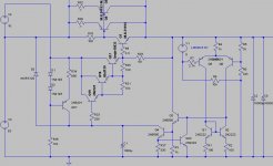
G.Kleinschmidt said:Here is a dynamic load test. The 100mA load (750 ohm resistor) is switched in and out of circuit at a rate of 1kHz. The load/no load level shift is about 400uV, indicating a “DC” output resistance of 4 milli ohms.
The key to this designs performance relies on the fact that the intrinsic output impedance (prior to the application of NFB) of a shunt regulator is very high. This means that an output stunt capacitor can provide plenty of HF attenuation, thus providing the dominant frequency compensation pole and still allowing the use of lots of negative feedback to regulate the output.
I’ve seen quite a few shunt regulator designs where it is evident that the designer has not recognised this fact, and they have done a silly thing such as trying to frequency compensate the gain block by rolling off it’s HF response. This “dominant pole” then has to compete with the frequency pole provided by the output shunt capacitor, thus needing to be set really low, killing the performance - especially the high frequency ripple rejection.
In simulation the design here does not begin to oscillate until I increase the ESR of the 470uF shunt capacitor to a huge 7 ohms, indicating a pretty reasonable safety margin.
Well that's my theory anyway, so I have designed this thing to prove it to myself and I will build it for fun.
Cheers,
Glen
Just printed out your schematic and will have a look at it. An interesting point you make above. This is a "super shunt" type design originated/patented from stax for there electrostatic phones I think. ie. using a CCS prior to the reg. J Carr has mentioned this on some posts. I wonder if they recognised this fact? maybe!
Glen could you do us a favour at some point when you have time, is do an impedance plot versus frequency ? I am interested in the relationship between output cap Z being lower or higher than the shunt reg Z. ie. Impulse (transient) power in the audio band.
Going to start on the beers soon.
Merry Christmas everyone!
Kevin
Fanuc said:Glen could you do us a favour at some point when you have time, is do an impedance plot versus frequency ? I am interested in the relationship between output cap Z being lower or higher than the shunt reg Z. ie. Impulse (transient) power in the audio band.
OK, I'll retrive the LTspice *.asc file in the next couple of days and post that up.
Cheers,
Glen
LC power snubber
Hi Klaus,
Back awhile (post 657) you mentioned adding a L-C snubber after the bridge to good effect.
Could you elaborate a bit about the design of this LC filter - it seems so obvious that it makes you wonder what other "gems" have also just fallen into dissuse.
Hi Klaus,
Back awhile (post 657) you mentioned adding a L-C snubber after the bridge to good effect.
Could you elaborate a bit about the design of this LC filter - it seems so obvious that it makes you wonder what other "gems" have also just fallen into dissuse.
Hi James,
this LC-"snubber" is a bit tricky and has only little figure of merit in simple circuits, if any.
It must be very carefully tuned (WRT frequency, Q and impedance), it then effectively shifts ripple to higher harmonics and keeps peak-to-peak ripple voltage lower, compared to a circuit with the same overall filter capacitance but without the inductor (which carries no DC, a nice feature). And it can be cascaded to do even more so.
All of which is of no worth (or even a bad thing) when there is no post filter with a steep slope, because power supply ripple rejection of amps tends to decrease with rising frequency, usually with a first order slope. The post filter might be passive (LC) or an buffered filter (source or emitter follower), with something like a 3rd order Bessel characteristic.
This make it obvious that only few circuits would see a net improvement with this, given the overhead. That's why you won't see it often in the industry, it has too many disadvantages to be considered universally useful.
Klaus
Hiii Bob
Hiii
I am newbee in DIYAudio (1 year )
little confuse about grounding
My amp system
---- + -----I---I --- (+,0) -- I-----I --- + I-------- I
---- G? . . . I T I . . . (G?) -- I PSU I --- - I Channel I
---- - ----- I__I --- ( -,0) -- I____I --- G I________I
Maybe i need a simple direction from you
is PSU need grounding from cable ?
If i look some PSU their connect just from transformer
(+, 0, 0 and - ) but if we use cable and plug theres
3 way cable +, 0 and ground
Is this ground need to connect ? (From Cable to PSU)
If it is connect must i add a resistor in there ?
I use 6pcs 10000uf 80V and bridge rectrifier 32a 200v
for 45VDC
really need your help
regards, jeffry
Hi Jeffry,
Sorry. You have not provided enough information.
There are many different types of power supplies. Each type of power supply might connect to the transformer in a different way than some other types connect to it.
Below is a link to a web page that has diagrams of how some types of power supplies and transformers are wired:
http://sound.westhost.com/power-supplies.htm
From your words and diagrams, it looks like you are talking about the "center tap" wire, on the 'secondary' side of the transformer. And you are naming that wire "Ground".
Often the center tap IS used as a 'ground reference' voltage for a PSU [which might be typical for some types of dual (i.e. +/- voltages) power supplies]. But sometimes the center tap is not used at all, or is used differently.
If your PSU makes two equal and opposite + and - DC voltages, then your center-tap wire 'probably' IS used as the PSU's ground reference voltage. But where and how that center-tap wire connects would depend on how you want to design your grounding scheme. (Maybe you should do some searches for 'star ground'.)
The transformer's 'center tap' is not really a 'ground'. It is just the 'middle' voltage, between the voltages of the two outer secondary windings' wires.
For example (NOT for YOUR power supply; only an example), you 'could' pick ANY one of the secondary wires, and call that wire the "ground". You COULD even CONNECT any one of the secondary wires to the real 'earth ground'. ONLY the voltage DIFFERENCE between the wires is important. Example: a "25-0-25" transformer could ALSO be used as a 0-25-50 transformer.
In electronics school I learned the equivalent circuit for an active device, like a transistor.
In this equivalent circuit the feeding power supply rail was always considered a shortcut for signals, hence the signal the transistor ( or any active device) handles goes through the supply to ground, i.e. the supply is equal to ground for signals.
I hope I can explain this clearly, but since than I realised that for any kind of stage to work properly, the supply has to be a shortcut for any signal.
So, like mentioned before, the VAS of any amp needs it’s own very well decoupled powerlines, or its powerline currents will interact with the larger currents from the output stage when powerlines are shared.
Same applies for the output stage, signal currents in de powerlines will interfear with the charging current peaks of the (also not so perfect) electrolytic capacitors.
Like said before, splitting these capacitors (CRC) and their grounding points will make things a lot better: the active stage sees a better shortcut to ground for signals, and the C connected to the rectifier handles the charging cycles with less interference with the signals through the other C.
Hence we have to realize that the signals of each active stage has to travel through the powersupply with the smallest resistance possible and without interfering each other.
This also explains why the quality of the used capacitors is more important than the value.
Dick
Here is a basic simulation schematic of the regulated +/-45V power supply I have designed for the power output stage of one of the three monster amps I am currently working on.
The amplifier is question is rated at 800Wrms into 1 ohm (40V peak) with a bias current of 5A for class A operation to 200Wrms into 4 ohms. Output current will be hard limited at 100A, providing full amplitude drive into a load resistance of 0.4 ohms.
Only the positive half of the regulator is simulated, the negative half being identical except that polarised components are inverted and the transistors are swapped for their N and P channel complements.
The design is unusual in that, while having a very high loop gain and therefore high (far better than required) DC precision, global negative feedback is not utilised to produce a low output impedance, as massive over compensation is used.
Attachments
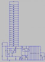
The series pass element consists of twenty MJL21193 PNP transistors in a CFP arrangement with one MJL21194 NPN driver transistor.
The CFP provides a lower output impedance than a straight emitter follower due to the local NFB loop.
The 20 parallel series pass devices ensure that the output impedance does not rise significantly at high load currents due to beta droop.
Q17, Q18 and Q19 form a triple emitter follower driver for the CFP.
Transistors Q5 and Q6 form the error sensing long tail pair, comparing a fraction of the output voltage developed across R5 against the reference diode potential.
Q1 and Q2 form a current mirror load for the LTP and Q3 and Q4 form a buffered VAS, resembling a common audio amplifier circuit.
Q21 is a 1mA constant current load for the VAS. C1 is the frequency compensation capacitor and the VAS current is limited to 2mA by Q22.
This results in a maximum push-pull charge/discharge current for C1 of +/-1mA, giving the global loop regulator a response .001/1000e-6 = +/-1volt per second.
This response is so slow that it ensures the regulator loop does not “fight” the audio signal current to keep the output voltage constant and provides unconditional stability into the excess of 20,000 uF of filter capacitance on the output (2 X 10,000uF + 1000uF + 100uF + 10uF + 1uF + 0.1uF).
Attachments
- Status
- This old topic is closed. If you want to reopen this topic, contact a moderator using the "Report Post" button.
- Home
- Amplifiers
- Solid State
- Bob Cordell Interview: Power Supplies