Hmm
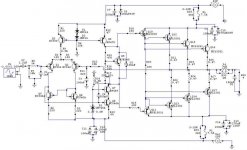
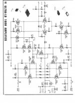
Somewhere I have seen this circuit but I can't quite place it....I just wonder what would happen to the bias of Q3 if Q6 were to saturate. Perhaps a seperate bias for Q3 and Q6 would make this a non-issue?
Just curious, what would be the difference if you replaced Q8 with a PNP type, use Q5 as the source and Q4 as the mirror, drive the emitter of Q7 with the emitter of Q8(PNP) as a common base VAS instead of a cascode VAS? I have done this and it sounds great, may reduce miller effect but I haven't built a casode VAS to compare. Any thoughts?
CBS240 said:Hmm
Somewhere I have seen this circuit but I can't quite place it....I just wonder what would happen to the bias of Q3 if Q6 were to saturate. Perhaps a seperate bias for Q3 and Q6 would make this a non-issue?
Q6 never saturates. That's the reason R1 and R12 have different values. The main idea is that Q3 and Q6 should have the same bias.
CBS240 said:Hmm
Just curious, what would be the difference if you replaced Q8 with a PNP type, use Q5 as the source and Q4 as the mirror, drive the emitter of Q7 with the emitter of Q8(PNP) as a common base VAS instead of a cascode VAS? I have done this and it sounds great, may reduce miller effect but I haven't built a casode VAS to compare. Any thoughts?
It would be a different design !

haven't tried that, so i can not comment.
But, you should always take into considaration the absolute phase of the signal (0 deg, or 180deg.) so, you won't end up with possitive feedback.
Re: Douglas
As long as the quiescent current remains below 80mA per transistor it's fine (already tested....).
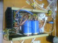
TomWaits said:Looks a little lite on the Heatsink side of things but looking good.
Shawn.
As long as the quiescent current remains below 80mA per transistor it's fine (already tested....).
and some specs:
145W @8 Ohms (20Hz to 20KHz)
268W @4 Ohms (20Hz to 20KHz)
The transf. has a 2x40.5V secondary, and the voltage on the caps is 54.9V with the amp idling.
At full power the voltage on the caps drops to 53V @8 Ohms and to 52.4V @4 Ohms.
It's the benefits of Overengineering!
145W @8 Ohms (20Hz to 20KHz)
268W @4 Ohms (20Hz to 20KHz)
The transf. has a 2x40.5V secondary, and the voltage on the caps is 54.9V with the amp idling.
At full power the voltage on the caps drops to 53V @8 Ohms and to 52.4V @4 Ohms.
It's the benefits of Overengineering!
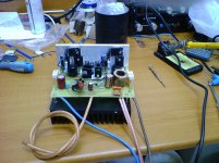
Attachments
Leolabs said:Hi Johnny1!Have you match the output BJTs???
Of course i have them matched!
Not only the output BJT's but also all the complementary pairs.
The differential pair and the current mirror BJT's are also matced pairs.
Onra said:Hi,
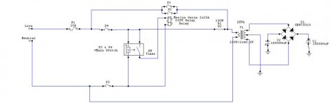
are you sure about the position of the main switch in the soft start schematic?
How do you manage to switch off?
Regards Onra
S3 and S4 switch on or off simultaneously.
The timer and the bypass relay WILL turn off, because the Neutral side is "open" by S3
I've simulated similar and found out that you can make Q6 saturate quite easily by driving the amp into clipping. This then makes Q6 steal enough current through the base to keep Q3 from working. A simple cure with little drawback is to put a resistor in the base of Q6 to limit it. Try 470R
I can't resist... A few comments as the amp has some minor flaws.
1, as jaycee already said, a basestopper to q6 is mandatory, it's sad how many published schematics forgot this one. Leaving it out can destroy your speakers...
2, Connect r7 to the other side of r8, this reduces DC-offset as the amps gets better balanced.
3, c8 must be a typo, you can't really put a permanent capacitive load to the amp ? This will ask for resonances in combination with L1.
L1 = 7uH ? Very big ! Use a much smaller value here (<1uH) and place a Zobel on the other side of the coil, skip c8...
4, a 2 diode ccs is nearly the worst ccs possible, consider a zener or led here. (or replace r4 with another ccs)
Mike
amplifier nice?
Hello gents
This is the very SAME amplifier published by Silicon Chip in 2002, called
by them as Ultra_D 100W amplifier...
Very minor differences, for example CCS is done with another BC556
instead of two diodes or LED. There is also no base stopper on Q6
and the cap at the output loading the speaker is the same. The coil
L1 is 6.8 uH not too distant from 7 on this schema.
The BIG difference (This is a laugh) is the upper output transistors
on Ultra-D schema are PNP (MJL1302) the lower ones NPN. How
is this for a difference?
Needless to say the collectors of both pairs of outputs are tied up
to (each two) 4 common 1.5 ohm resistors.
I asked for the layout to Johnny 1 but I don't need it, I have it
from the Ultra-D, thanks.
- Status
- This old topic is closed. If you want to reopen this topic, contact a moderator using the "Report Post" button.
- Home
- Amplifiers
- Solid State
- My little beast is getting ready..