What do y'all think of Steven Gunderson's approach?
Note that this is the technique used by Rotel in their RB1090 power amp., and Randy Slone in his designs.
Also available as:
'A Topology to Linearize Miller-Effect Compensated Amplifiers'
JAES Volume 32 Number 6 pp. 430-434; June 1984
An additional topology to Miller-effect compensated amplifiers, which reduces high-frequency distortion, is described. The addition is implementable in discrete or integrated circuits, with little or no additional complexity required in designs incorporating short-circuit protection. This topology is effective in reducing distortion to frequencies greater than 10 MHz. The greatest effect is achieved in power amplifiers with push-pull output stages.
Author: Gunderson, Steven J.
The Rotel's schematic looks like a cascoded VAS, but towards output node, not static cascode.
The patent's intention seems to isolate the output stage (distortion+nonlinearities) from affecting the input/previous stage by putting a common base transistor between output stage and VAS.
John Curl have the same intention, but doing it by putting a Mosfet predriver.
The patent's intention seems to isolate the output stage (distortion+nonlinearities) from affecting the input/previous stage by putting a common base transistor between output stage and VAS.
John Curl have the same intention, but doing it by putting a Mosfet predriver.
lumanauw said:The Rotel's schematic looks like a cascoded VAS, but towards output node, not static cascode.
Actually, Rotel's implementation is identical to Gunderson's-in his JAES paper.
ITEM # PCBV-2 Lang 20W Mosfet Power Amplifier
From Audio Amateur Issue 2/86. Lang 20W single-channel Mosfet power amplifier. 5-11/16" x 6-1/16". 1 lb. $21.40
http://www.audioxpress.com/bksprods/pcbs/solidstate.htm
Uses lateral FET outputs, fully comp, in to out.
From Audio Amateur Issue 2/86. Lang 20W single-channel Mosfet power amplifier. 5-11/16" x 6-1/16". 1 lb. $21.40
http://www.audioxpress.com/bksprods/pcbs/solidstate.htm
Uses lateral FET outputs, fully comp, in to out.
djk said:Lang 20W Mosfet Power Amplifier
Does it use the same compensation?
mikeks said:
Does it use the same compensation?
No. The Lang is classic: diff input bipolar, cascoded Vas, SK133/SJ48 output stage. Only comp is 68pf C-B on input side of diff input pair, probably because of the low ol gain (heavily degenerated input pair).
Jan Didden
mikeks said:
Actually, Rotel's implementation is identical to Gunderson's-in his JAES paper.
I'm curious as to when the JAES paper was published (and where I can get a copy of it to read ) I've been using this form of cascode for years after seeing it used in the GAS Ampzilla II (and IIa). The patent was granted in April of 1985, and I believe The Great American Sound company was dead and gone in 1981...
Sonically This is a great circuit. It is a lot purer in the highs and it also removes a bit of a resonant heavyness noticed most at the bottom end of the mail voice. To my ear it sounds right.
Mike.
janneman said:
No. The Lang is classic: diff input bipolar, cascoded Vas, SK133/SJ48 output stage. Only comp is 68pf C-B on input side of diff input pair, probably because of the low ol gain (heavily degenerated input pair).
Jan Didden
hit us with schm ,just for fun
mikeks said:What do y'all think of Steven Gunderson's approach?
Note that this is the technique used by Rotel in their RB1090 power amp., and Randy Slone in his designs.
Also available as:
'A Topology to Linearize Miller-Effect Compensated Amplifiers'
JAES Volume 32 Number 6 pp. 430-434; June 1984
An additional topology to Miller-effect compensated amplifiers, which reduces high-frequency distortion, is described. The addition is implementable in discrete or integrated circuits, with little or no additional complexity required in designs incorporating short-circuit protection. This topology is effective in reducing distortion to frequencies greater than 10 MHz. The greatest effect is achieved in power amplifiers with push-pull output stages.
Author: Gunderson, Steven J.
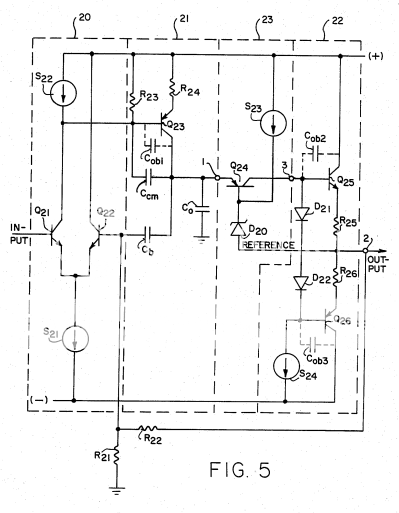
In fig. 5 the emitter of Q24 'common base transistor' is at constant voltage against output, so Q24/Q25/Q26/diodes/CCSs circuit is a follower by its 'lovemaking' definition, it just consumes considerable DC comparing to classic followers.
Aside from this I see two poles and a local phase lead back to LTP, so a transfer function has 2 poles and one zero, not so uncommon I think.
Agreed? Please Mike don't answer just 'Nope...'
I would be interested on load stability of such a circuit.
best regards
Adam
just some random musings:
An entertaining view might be that the “cascode” transistor Q24 implements a unity gain local voltage feedback around the output stage
With the hi Z VAS output driving the emitter it is more readily viewed as a “cascode” because no current gain is available and only the input current at the cascode emitter is applied to the output stage base – as freq rises the local VAS miller Cm (or gnded Co) reduces the input Z at the "cascode" Q24 emitter and the output/”cascode” loop gain rises
Looking at the circuit as local output stage feedback loop the question becomes why no current gain as you can have with other local output stage feedback loop circuits?
Perhaps this approach is easier to compensate?
Since it only has voltage gain the only distortion that can be addressed is the Vbe variation of the output – significant in Class AB but not really a problem in Class A
from US4511857
[ anyone know who "owns" the copyright on a US patent? I assume that copying a single image with attribution is "fair use" in any event ]
Re: just some random musings:
Correct.
Indeed, as far as the minor loop is concerned, the so-called 'cascode' transistor is merely an emitter follower with respect to voltage fed back from the output stage.
jcx said:An entertaining view might be that the “cascode” transistor implements a unity gain local voltage feedback around the output stage
Correct.
Indeed, as far as the minor loop is concerned, the so-called 'cascode' transistor is merely an emitter follower with respect to voltage fed back from the output stage.
Re: Then again..
Kind of. Through R22 and Cb there is a local positive feedback with gain rising with frequency, which can be problematic unless Co is much higher. I doubt if all this was designer's intention...
mikeks said:...it could well be urgued that the minor loop possess two paths in parallel..
Kind of. Through R22 and Cb there is a local positive feedback with gain rising with frequency, which can be problematic unless Co is much higher. I doubt if all this was designer's intention...
Hi, JCX,
Interesting POV
If the voltage at emitor of Q24 (point 1) reflect the output voltage at point 2, what is actually happening in this configuration?
-In fig.1, there is a feedback line from output (2) to the middle of box "OFICC".
-In fig.6, this OFICC reduces the distortion.
Both these figures to me seems that this OFICC is working like Error Correction (EC), but looking at fig.5, I don't know how EC can happen between point 1 up to point 2 ?
In the writings of the patent, column7 section 50-55, the author said that this configuration does not do anything to the non-linearities, but only isolating point 1 from point 3 (fig 5). Is the effect can be so drastical?
Point 2 is distanced by zener D20 + Vbe drop of Q24. This means the AC voltage (not DC) is the same between point 2 and point 1.
What's the purpose of doing this?
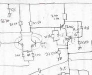
If the intention is to isolate point 3 from point 1, a simple ordinary VAS cascode like below should do the same thing.
In the example below the VAS transistor is cascoded by 1 green LED drop//with 0.1 cap. This should do the isolation too, isn't it?
What's the purpose of doing this?
If the intention is to isolate point 3 from point 1, a simple ordinary VAS cascode like below should do the same thing.
In the example below the VAS transistor is cascoded by 1 green LED drop//with 0.1 cap. This should do the isolation too, isn't it?
Attachments
- Status
- This old topic is closed. If you want to reopen this topic, contact a moderator using the "Report Post" button.
- Home
- Amplifiers
- Solid State
- Gunderson compensation..