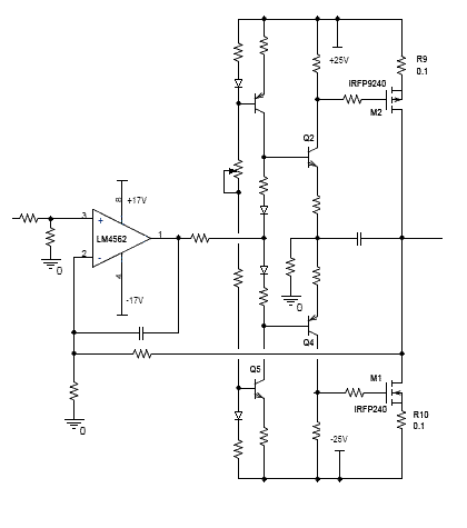
Mine is an opamp driven (LM4562) Sziklai pair biased with a pair of diodes loaded by a current source and a current sink.
The idea is to build a dorm-room amplifier that doesn't generate much heat and that gives its best distortion figure at arround 2 to 8 Wrms. Simulation results give less than 0.001% distortion for all the audio spectrum at this range. Simulation does not use any compensation part but a 100pF silver-mica between the two bases.
I'm happy to see that yours worked. I may build one in a month or so and post the results here since this thread really deters one from trying hibrid Sziklai arrangements.
djk said:
Be aware this configuration suffers from serious crossover spikes due to the fact that the output device transitioning from cutoff to conduction must have its gate capacitance rapidly charged in order to reach threshold voltage, and this in turn implies a large current (gate capacitance is in the nF range) for a brief period that must be supplied by the drivers.
In practice what one sees is a feedback induced step in the driver's base and ringing until the loop stabilizes.
On simple way to overcome this is connecting a resistor from gate to ground for each output device so as to ensure it never reaches full cutoff, but the idle current is hard to stabilize and in practice results in a quasi class A mode with heavy disipation.
I posted here a more complex bias arrangement that works nice and have made amplifiers in the low 0.001% THD range that sound good.
Rodolfo
Member
Joined 2009
Paid Member
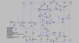
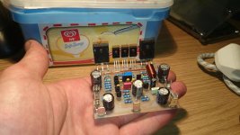
I am working at the moment on the mosfet CFP output stage amplifier, the first prototype is working fine, sound is very delicate but I must spend some more time on it to learn a bit more about CFP output stages.
The schematic is simple. If someone can give me some more advices/ideas about improvements would be nice.
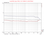
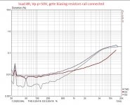
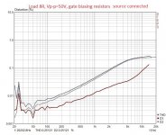
The config from post 82 is looking nice. The spice is throwing thd around 0.005%@10kHz@ 50Vp-p wchich looks ok for me but my board is throwing around 0,5% thd at the same conditions
The schematic is simple. If someone can give me some more advices/ideas about improvements would be nice.
The config from post 82 is looking nice. The spice is throwing thd around 0.005%@10kHz@ 50Vp-p wchich looks ok for me but my board is throwing around 0,5% thd at the same conditions
Attachments
Last edited:
Member
Joined 2009
Paid Member
Looks nice !
... usually for me, for a CFP, the 'local' feedback from output drain to driver emitter should be connected directly and then isolated from the amplifier output by a resistor. You have a different arrangement, more like common emitter driver and common source power device. Well - just a thought anyhow.
... usually for me, for a CFP, the 'local' feedback from output drain to driver emitter should be connected directly and then isolated from the amplifier output by a resistor. You have a different arrangement, more like common emitter driver and common source power device. Well - just a thought anyhow.
The spice is throwing thd around 0.005%@10kHz@ 50Vp-p wchich looks ok for me but my board is throwing around 0,5% thd at the same conditions
Since most THD comes from output stage try to make these changes:
- omit R22, R33
- put 50 Ohm parallel with 10 uF film cap between emitters of Q11, Q13
- connect R31, R32 to sources of M1, M2, not to rails
- lower degeneration resistors R20, R21 to 22 Ohm or less
- use low Z degeneration resistors to bases of Q11, Q13
- higher the voltage gain of VAS/mirrors by lowering emitter resistors
- lower R8 to 10 kOhm
- lower R1, R2
- connect 0,1 uf parallel to R16
- C13 to 1 uF
LC
I have made the changes today but without drivers connected to nfb (with single resistors) there is no way of biassing the mosfets, with bjt standard CFP would be no problem but mosfets they not biassing up at all, vgs is going to 0V slowley. In spice it is working fine.
But I have desoldered C12 cap from VAS stage (wima mks2 100nF) and distortions dropped a lot. Maybe few more hours and i will call it an amp.
I have connected gate resistors to the rail and to the sources, It may be helpfull for someone.
BIG THANKS AGAIN
Attachments
Hi,
I have found this CFP : (but Q18 / Q19 are inverted compared to normally seen)
http://www.diyaudio.com/forums/attachments/sito-audio/397410d1391375434-tssa-v1-7-tssa-v17-sch.pdf
http://sitosite.dk/amps/TSSA-01300712.pdf
It is possible to use this CFP in VSSA LATFET ?
It is possible to use more than one push ?
Thanks
Last edited:
Since most THD comes from output stage try to make these changes:
- omit R22, R33
- put 50 Ohm parallel with 10 uF film cap between emitters of Q11, Q13
- connect R31, R32 to sources of M1, M2, not to rails
- lower degeneration resistors R20, R21 to 22 Ohm or less
- use low Z degeneration resistors to bases of Q11, Q13
- higher the voltage gain of VAS/mirrors by lowering emitter resistors
- lower R8 to 10 kOhm
- lower R1, R2
- connect 0,1 uf parallel to R16
- C13 to 1 uF
In this configuration it is nor a CFP !?
You could just be looking at horrendous inductive rail coupling. One way to test for that is to measure the amplifier with the FETs biased optimally, then to take another measurement with the output stage biased into class A.
Obviously you'd have to do this at a significantly lower output power, but if there's a tremendous difference between optimum and class A then you've found a problem.
Obviously you'd have to do this at a significantly lower output power, but if there's a tremendous difference between optimum and class A then you've found a problem.
LC
I have made the changes today but without drivers connected to nfb (with single resistors) there is no way of biassing the mosfets, with bjt standard CFP would be no problem but mosfets they not biassing up at all, vgs is going to 0V slowley. In spice it is working fine.
Interesting really. To properly bias the mosfets current through R31, 32 has to be high enough (6-8 mA) so single Ree=56 Ohm between driver's emitters should not cause the problem. Maybe VAS stage cannot deliver the current to the drivers therefore its bias should be set higher. Something's not right here.
Hi,
I have found this CFP : (but Q18 / Q19 are inverted compared to normally seen)
Not inverted, Q18-U1, Q19-U2 act as BJT-Mosfet Darlington in VAS stage. This is basic TSSA topology in expanding mode, having VAS power stage in double function, as voltage amplifying stage and as load current delivery stage. Since CFP acts like a curent source/sink (high output impedance in open loop) voltage gain curve is very much load impedance dependable, so quite a task for feedback error control to lower distortions. High open loop gain and stability are certainly welcome here but in reality things are in quite opposite manners.
- Status
- This old topic is closed. If you want to reopen this topic, contact a moderator using the "Report Post" button.
- Home
- Amplifiers
- Solid State
- Ever made a MOSFET CFP/Sziklai that works?