In general, you don't want to allow the base emitter to go into reverse breakdown. I'd clamp it lower than the expected reverse breakdown voltage.
That's why the 2SC2878 muting transistor is special. It is designed for high reverse emitter base voltages, and they still fail. They tend to get leaking in funny ways that test good.
-Chris
That's why the 2SC2878 muting transistor is special. It is designed for high reverse emitter base voltages, and they still fail. They tend to get leaking in funny ways that test good.
-Chris
richie00boy said:Interesting. What about the EF Type II output stage where the driver can reverse bias the output? They seem to survive OK - lots of Leach amps and AKSA amps and others and you never hear of them breaking.
Well, first of all, drivers and output transistors are more robust so probably they can survive higher reverse currents - the outputs for sure. Also, if they are driven by a Vas stage, the current is also inherently limited which may save them.
Jan Didden
Hi,
Vbe max is the limit when driven into saturation in the normal direction.
I would treat that as an absolute limit unless the manufacturer is more forthcoming. Maybe 70% of absolute for normal operation when saturated.
The reverse (-Vbe for NPN and +Vbe for PNP) voltage will be different and could be much smaller.
How about adding a parallel diode to short the reverse current past the junction and thus produce a volts drop across the preceeding resistor.
AndrewT said:Hi,
Vbe max is the limit when driven into saturation in the normal direction.
I would treat that as an absolute limit unless the manufacturer is more forthcoming. Maybe 70% of absolute for normal operation when saturated.
The reverse (-Vbe for NPN and +Vbe for PNP) voltage will be different and could be much smaller.
How about adding a parallel diode to short the reverse current past the junction and thus produce a volts drop across the preceeding resistor.
The reverse is normally around -7 (NPN) for zenering to occur. But it is a very noisy zener.
There was a time when reverse biased B-E junctions were used as noise sources in test equipment.....
The forward is normally not a problem as long as the base current is not exceeded. What will happen is if you increase normal Vbe is that the Vc will get lower and lower until at saturation Vce will be just a couple of mV (in a small signal transistor). Actually, base current will then start to flow directly into the collector because the B-C junction becomes forward biased.
Jan Didden
The B-E junction of bipolar transistors acts like a zener diode when it's reverse biased. This means that it also has its own power rating and pulsed SOA curves like zeners, that unfortunately are not published in datasheets. In other words, it's excess dissipation or excess peak current what will damage a reverse biased B-E junction and not just the negative voltage itself.
By the way, I have tested some NPN switching power transistors to survive up to -1A of pulsed B-E breakdown current or -100mA DC without damage (no changes in Vbe or hFE happened). Small signal transistors seem to be quite fragile and easy to damage, though.
By the way, I have tested some NPN switching power transistors to survive up to -1A of pulsed B-E breakdown current or -100mA DC without damage (no changes in Vbe or hFE happened). Small signal transistors seem to be quite fragile and easy to damage, though.
Bad Ju Ju...
You can't limit the current; because you don't know what to limit it to. There are some BE junctions (gold doped maybe?... i can't remember) that are more fragile then others.
Manufcacturers don't provide data because you're not supposed to do it. Limit the voltage you apply... a 3.3V zener in series with silcon rectifier does the trick. You need the silicon rectifier to burn some voltage so you don't forward bias the zener during normal transistor operation.
")
You can't limit the current; because you don't know what to limit it to. There are some BE junctions (gold doped maybe?... i can't remember) that are more fragile then others.
Manufcacturers don't provide data because you're not supposed to do it. Limit the voltage you apply... a 3.3V zener in series with silcon rectifier does the trick. You need the silicon rectifier to burn some voltage so you don't forward bias the zener during normal transistor operation.
Hi,
Thanks for support.
I have two choices : (1) add a diode from emitter to base ; or (2) add a voltage divider before base , so base negative voltage would be limited to around -5V.
In the first case, i'd need additional resistor to prevent previous stage(opamp) from drawing excess current.
Regards,
Lukas.
Bazukaz said:Hi,
Thanks for support.
I have two choices : (1) add a diode from emitter to base ; or (2) add a voltage divider before base , so base negative voltage would be limited to around -5V.
In the first case, i'd need additional resistor to prevent previous stage(opamp) from drawing excess current.
Regards,
Lukas.
A diagram might help. Maybe it is already self-limiting? You have a base series resistor?
Jan Didden
Hi,
Thanks for help.
Here is the schematic. It is a high voltage amp , only one half of bridge shown.
I have now inserted a resistor divider before base of Q1 , but , i think it would be even better to use a base resistor and diode at emitter - base instead.
Regards,
Lukas.
Thanks for help.
Here is the schematic. It is a high voltage amp , only one half of bridge shown.
I have now inserted a resistor divider before base of Q1 , but , i think it would be even better to use a base resistor and diode at emitter - base instead.
Regards,
Lukas.
Attachments
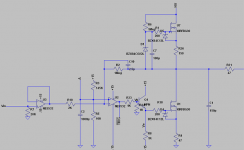
I would delete R34, it wastes half your drive voltage. A diode from E to B probably is best.
You could also put a diode in series with the protection zener on U1 so that the transistor E can swing down to the - supply which would avoid the problem altogether, but I don't know what the allowed neg voltage on the FET gate is.
If you can increase R33 to limit opamp saturation that would also be good.
Have you simulated this? How do the curves look for Vbe?
Jan Didden
- Status
- This old topic is closed. If you want to reopen this topic, contact a moderator using the "Report Post" button.
- Home
- Amplifiers
- Solid State
- Transistor base negative voltage