THis is my new construction I`ve been working on last two month..
Any suggestions before I start making pcb ?
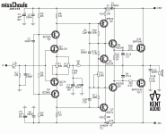
1.Input stage, iddle current 5.56mA.
2. VAS stage , iddle current 21.6mA.
3. Buffer stage , iddle current 35.1mA.
4. Output stage , iddle current 100mA.
Any suggestions before I start making pcb ?
1.Input stage, iddle current 5.56mA.
2. VAS stage , iddle current 21.6mA.
3. Buffer stage , iddle current 35.1mA.
4. Output stage , iddle current 100mA.
Attachments
Hi,
1, I wouldn't use trimmpots (P1, P2) in signal path, they increases noise
2, I would use IRFP9240 instead of IRFP9140
3, I would place a resistor in series with P3, because without it the output fets can blow up because of the high idle current if the trimmpot not adjusted properly
4, C7 looks to low value for me, I would use 2200uF or 3300uF cap here. that will give better bass reproduction
5, R14 and D2 are reversed in the schema. anyway I would use 1N4148 instead of 1N4004.
6, I would use only 100uF in place of C3-C4, and place the 1000uF caps on the psu rails yet near the output-mosfets drains.
Regards,
OK then ")
1) Trimpots: P1 is OK, P2, chose the best you can find as any problems with resistance of the wiper will make things behave badly.
2) IRFP9240 vs 9140, we've covered that before. Using 9240 as a complemet to 240 is a knee-jerk reaction, because they are NOT complements electrically - but you already know all that.
3) Put a resistor in series with the wiper of P3. This limits the maximum quiescent current and also stretches ot the regulation some so it is not so abrupt with wiper travel.
4) C7 is indeed relatively low in value. The problem here is not the low end cut off, but capacitor distortion. Caps have very low distortion as long as the AC component on them is low. Electrolytics can have pretty high distortion when large AC components are present. Because of this, they are routinely overdimensioned. The time constant of (R8||R9)*C7 must be quite large, if you want to limit subsonics, do it at the input by AC coupling.
5) 1N4148 are a bit too resistive and may not survive charging of C3 and C4 from zero, so 1N4004 or perhaps their fast recovery version UFD4007 should be used.
6) PSU rails at MOSFET drains indeed need some form of decoupling. 100uF in place of C3 and C4 would not be enough, your 1000uF parts there are better suited. In fact, ypu may even want to increase them, see below.
7) MOSFET driver stage must be powered AFTER the diodes, or you will lose Vgs - 0.7V off the rails at clipping. This is because the buffers need to drive the gates of the MOSFETs above the drains, as it is drawn now, this will not happen becayse the B-C junction will act as a clamping diode. In order to use the buffer on the other side of the diodes, you may need to increase C3 and C4 to account for buffer current, also decrease or even ommit R13 and R14.
8) Since you are using a buffer, you may not need as high a VAS current. Granted, higher VAS current improves it's gm, but you may get the same effect by using lower currents but, since currents are lower, you can use smaller, higher gain transistors.
9) Split C2 into two capacitors with ground in the middle. You could also make up a modulated cascode, but that gets a bit more complex.
10) Your zener diodes D3 and D4 are not really going to work as zener diodes at all! Consider this: the bias voltage between gates of the MOSFETs is about 6-7V, and is held near constant by the Vbe multiplier. The gate of each MOSFET can only swing up this bias voltage plus one diode drop with respect to the sources of the MOSFETs, because at that point one of the zeners becomes forward biassed and clamps the oposing gate to the source common point plus one diode drop. This will translate to maximum Vgs of about 6.5-7.5V. Even so, this may be too much. Keep in mind that there are no source resistors, 6.5-7.5V will completely saturate the MOSFETs, so while you have gate overvoltage protection, your output current is not really limited.
11) Q5 may slightly thermally overcompensate the MOSFETs + buffers, you may need a small resistor in it's emitter or a diode in it's collector, or you can carefully chose the values of R12 and P3 to provide a partial shunt for the VAS current, reducing the effective tempco of the Vbe multiplier.
12) What do R10 and R11 do?
1. 100uF is a small value for c3 and c4 becose vas+nput stage iddle current is over27mA!
2. IRFP9140 is better complementary to IRFP240(Look datasheet)
3.If P3 is not adjusted properly or broken, idle current of the output stage gets LOWER!
4.P1 and P2 are not in the signal path! They paralleled with the resistor (i missed it in the schematic).
are you drunk edi?
2. IRFP9140 is better complementary to IRFP240(Look datasheet)
3.If P3 is not adjusted properly or broken, idle current of the output stage gets LOWER!
4.P1 and P2 are not in the signal path! They paralleled with the resistor (i missed it in the schematic).
are you drunk edi?
I was waited for you ILIMZN !!!
-Q6 and Q7 are changed with the MJE340/350
-wath should I do with the zener diodes D3 and D4??
-R10 and R11 are for the local feedback of the vas stage (for lower distortion).
-there is a resistor paralleled with the P3(I missed it in the schematic)
-I`ll parallel both sides of the pot P2 for safety (good idea).
any other expert to comment????
Hi Bogdan,
edl is trying to help. Be nice.
edl is correct about a resistor in series with P3. If you adjust P3 to it's short position or low enough value, the bias current will become circuit maximum. This will not be good for you.
ilimzn already reminded everyone. Point was made.
We aren't all perfect and we all make mistakes. Accept them with grace please.
-Chris
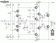
...See my point #7, R23 I believe was supposed to be connected with P3?
Local feedback in the VAS will reduce distortion but only in the VAS, you still get output distortion if present. It also reduces OL gain, which can be good or bad, depending on how you do it and how much you reduce it...
Local feedback in the VAS will reduce distortion but only in the VAS, you still get output distortion if present. It also reduces OL gain, which can be good or bad, depending on how you do it and how much you reduce it...
You still have the same problem with the EF driver stage (my point #7) and P3 as before. A little more concentration and a bit less impatience, perhaps?
Your zeners still will not work as zeners - and how did you chose the voltage? You could put them on the VAS side of the EF driver, as even now it is likely your EF driver will fry the 100 ohm resistors and perhaps itself if you short the output (te ony thing limiting current is the 100 ohm resistors, across a full supply rail...). C2 is still under a question mark, it does not really stiffen the cascode reference voltage, just transfers charge from positive to negative cascode and back.
Your zeners still will not work as zeners - and how did you chose the voltage? You could put them on the VAS side of the EF driver, as even now it is likely your EF driver will fry the 100 ohm resistors and perhaps itself if you short the output (te ony thing limiting current is the 100 ohm resistors, across a full supply rail...). C2 is still under a question mark, it does not really stiffen the cascode reference voltage, just transfers charge from positive to negative cascode and back.
- Status
- This old topic is closed. If you want to reopen this topic, contact a moderator using the "Report Post" button.
- Home
- Amplifiers
- Solid State
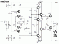
- my new construction (finall version-I hope so)