Hi, am a DIY but not an expert in amplifier design, I've built this amp but the highs are sounding harsh and bass is not sufficiently present. I have measured the output impedance to be 0.437 R, but stilll don't have anyy clue on how to smooth the high frequencies. Any help would be welcome. Thanks
Attachments
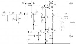
I don't see what R1 and R2 are for since there are onpy one output transistor per rail. You may try to remove them.
Use a trimpot instead of R11 in order to ragulate the idle current.
The schematic is very similar to Project 3A at Rod Elliot's site www.sound.au.com. Go there and read the description of the project.
Good luck.
Use a trimpot instead of R11 in order to ragulate the idle current.
The schematic is very similar to Project 3A at Rod Elliot's site www.sound.au.com. Go there and read the description of the project.
Good luck.
sparkybg said:I don't see what R1 and R2 are for since there are onpy one output transistor per rail. You may try to remove them.
Hi,
Under no circumstances should you remove R1 and R2,
they are essential for thermal stability.
The bias must be accurately set for low distortion.
see here :
http://www.dself.dsl.pipex.com/ampins/dipa/dipa.htm
edit : with feedback output impedance should be much lower than 0.4R.
I'd also add an output inductor with a 3.3R resistor in parallel for damping.
") /sreten.
/sreten.sreten said:
Hi,
Under no circumstances should you remove R1 and R2,
they are essential for thermal stability.
The bias must be accurately set for low distortion.
see here :
http://www.dself.dsl.pipex.com/ampins/dipa/dipa.htm
edit : with feedback output impedance should be much lower than 0.4R.
I'd also add an output inductor with a 3.3R resistor in parallel for damping.
UPS!!!
 Right! Do not remove them. A little lower values, down to 0.22ohm may be used, but they must be there.
Anyway I don't think they are the problem. Check the idle current. It must be at least 30mA per output device.
If you have access to oscilloscope you can check for high frequency oscillations. If the amplifier gets hot even when idle, this is often a symptom of oscillation. Adding emmiter resistors in VAS and DIFF stage may help a little with oscillations also I think.
zeus_threat said:Hi, am a DIY but not an expert in amplifier design, I've built this amp but the highs are sounding harsh and bass is not sufficiently present.
Any component of your audio chain could be responsible of harsh sound and I guess that any long-distance analysis would probably be useless.
Anyway - I would suspect wrong bias current and resulting crossover distortion. Try to measure voltage drop across end-stage emitter resistors. And if you happen to have test CD with 1kHz sinus, try it. You must not hear any sound from the tweeter, provided there is at least 12dB/oct high-pass.
Hi Adam,
oh, you have also built the amplifier zeus_threath presented a schematic on?
How does it perform?
About the capacitor across a Vbe multiplyer, I can not for sure suggest exact value for the schematic presented here which would be ok because it depends on several things, I found that some leave it out while other use it, where some use the same value as you, others even much higher values, 10 uF and up.
I would say it depends on how much the load seen by VAS in following stage varies by signal and load and think it through in combination with trial n' error what would suit your ears, and eyes when looking at measuring results!
What I try to say is that the upper and lower half might not even necessary show up consistent load which becomes more crucial at higher frequencies in some cases.
BTW I agree also with you that input diff could be degenerated of course too.
Oh, and one another thing when I look closer at the schematic is b-e resistor for output transistors, I don't know what transistors are used for the outputs but one should find out if approx 3 mA is enough to pull off those transistors, as cross conduction comes to my mind.
Cheers Michael
Thanks Michael
I meant Vbe multiplier in general, not in this very example. Send me mail if you want to see my circuit. I was looking for some formulas and suggestions at diyaudio and still don't know which is optimum. Polypropylene is OK?
Do you think differences can be easily hearable? I did not change caps and compare, should I?
regards
P.S. sorry for a bit off topic
Thanks for the help
Hi, i'd like to say thanks to everyone for the help. I'll try the emitter resistors plus the tests you mentionned. I agree about the signal polarized capacitors. Actually its a bipolar capacitor thats in place for C3. I'll update the schmeatics with the actual transistor nos used. R11 is in fact a 4.7K trimpot and the amp is biased to 100ma and i can tell you that it gets hot while playing and warm with no signal. The amp is in fact a modified P3A with active current sources and current mirrors not present in the P3A.
I have also tried emitter follower output configuration but the compound pair seemed to give better results. Additional info would be welcome
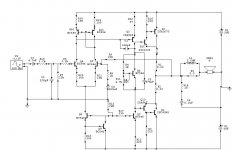
I think that you have choosen very bad resistor values. Differential pair is biased by 2mA, what makes voltage drop on R18&19 about 0.1V what is not enough, I recomend value about 1V (1k for R18&19). Also you have choosen very low bias for VAS stage (just 3mA). I've used with good results current about 10mA (R12=65R and R22=100R), but you have to watch power dissipiation of VAS stage according to your supply voltage.
These are just values I used with good results in very similar topology amplifiers)
These are just values I used with good results in very similar topology amplifiers)
DarkOne said:I think that you have choosen very bad resistor values. Differential pair is biased by 2mA, what makes voltage drop on R18&19 about 0.1V what is not enough, I recomend value about 1V (1k for R18&19).
This would not work, as it will result in too much input voltage bias for a single-transistor invertor Q3. Vbe of Q3 + voltage drop on R22 will give you only about 0.8V and you'll need to give some space for a voltage swing at that point as well - to close Q3 completely it would need at most about 0.4-0.5V. With a voltage drop on R18/R19 at 0.1V it would leave only 0.3V for Vce of Q10 - not much to play with...
Cheers
x-pro
x-pro said:
This would not work, as it will result in too much input voltage bias for a single-transistor invertor Q3. Vbe of Q3 + voltage drop on R22 will give you only about 0.8V and you'll need to give some space for a voltage swing at that point as well - to close Q3 completely it would need at most about 0.4-0.5V. With a voltage drop on R18/R19 at 0.1V it would leave only 0.3V for Vce of Q10 - not much to play with...
Cheers
x-pro
With values I wrote, there's a voltage drop of 1V on R18, but the base of Q3 see voltage on R18 + Vbe of Q10. The truth is that I haven't used current mirror to load diff stage (and I don't use it at all). If you can remove the current mirror, there should be another changes needed for diff stage biasing. 1V is the minimum voltage, to find out where yhe problem is with harsh sounding, you can tweak values and find which ones are best for you (I currently use voltage drop of about 6V)
Regards
Robo
DarkOne said:With values I wrote, there's a voltage drop of 1V on R18, but the base of Q3 see voltage on R18 + Vbe of Q10. The truth is that I haven't used current mirror to load diff stage (and I don't use it at all)....1V is the minimum voltage, to find out where yhe problem is with harsh sounding, you can tweak values and find which ones are best for you (I currently use voltage drop of about 6V)
But you did find it necessary to suggest 1V voltage drop on current mirror degeneration resistors? And state that this is the minimum? REALLY? Could you enlighten the rest of us as to why?
Normally about Vt (~25mV) is enough for a drop on the current mirror degenerators. If you can put the current mirror BJTs close enough, that should be perfectly enough for good thermal tracking and symetry. Also, you will still be able to turn off Q3 (although there are other things that could be done here).
Degeneration of ths input pair requires increasing the tail current for gm to remain equal, also with it the open loop gain. Of course, one could reduce open loop gain by input stage degeneration but you soon get to a point where this is not the bottleneck any more.
I would seriously think about reducing the emitter resistor of Q3. The potentially good thing of an emitter resistor there, along with some protection from deep saturation of Q3, is a lower open loop gain (may help with TIM and stability) but not less nonlinear. The actual gain of the VAS depends on it's collector load, that being the output stage. This is hardly linear. If you need to reduce VAS gain, the better approach might be to give it a more defined load by including a resistor from Q3 collector to ground. This lowers gain but also linearizes it as now the load impedance always has this resistor in parallel, which means it's fluctuations appear smaller WRT to the mean value.
You may extend bandwidth by increasing VAS current, though be mindful of the total dissipation for your transistors. Your differential stage certainly supports higher VAS currents, 10mA should be no problem.
I would strongly recomend getting a scope and checking the amp output with a load that at least tries to simulate some reactance. CFPs have many virtues, but also a propensity to oscillate. What you describe seems like a case of that. The prpblem is, they are not trivial to compensate. Here I am hesitant to give you any pointers as I don't think I can give you sensible ones like this 'remotely' especially without seeing at least a few oscillograms.
You might also try some form of lead/lag compensation. I have found that you can often reduce the dominant pole cap (C-B of Q3) which is a good thing to do in general (improves PSRR), but this I would think about when the basics are done
Ilimzn, please discuss with x-pro and try to find out some right value. There is nothing wrong with at least 1V volage on R22, even if 65mV is enough for you. Yo simply can't go wrong with higher value. Please use 65mV bias if your amp has not enough harsh sound.
I don't currently use current mirror, but I used it in the past.

I don't currently use current mirror, but I used it in the past.
BECAUSE I CANCould you enlighten the rest of us as to why?
Hi,
Biasing the amplifer to 100ma is incorrect, you will get gm doubling.
Read the Self article I posted earlier.
It shows the critical parameter for low distortion is the voltage
across the emitter resistors not the current. The value of the
emmiter resistors + the voltage drop required determines the
correct bias current.
The resistors can be reduced to as low as 0.1R, typical is 0.22R, 0.47R is too high.
A CFP (complementary follower pair) output stage correctly biased runs cool.
The voltage across the Vbe multiplier should be very near 1.3V.
I'll have to check my book at home for the exact voltage drop
across the emmiters resistors, the article doesn't give it.
/sreten.
Biasing the amplifer to 100ma is incorrect, you will get gm doubling.
Read the Self article I posted earlier.
It shows the critical parameter for low distortion is the voltage
across the emitter resistors not the current. The value of the
emmiter resistors + the voltage drop required determines the
correct bias current.
The resistors can be reduced to as low as 0.1R, typical is 0.22R, 0.47R is too high.
A CFP (complementary follower pair) output stage correctly biased runs cool.
The voltage across the Vbe multiplier should be very near 1.3V.
I'll have to check my book at home for the exact voltage drop
across the emmiters resistors, the article doesn't give it.
/sreten.- Status
- This old topic is closed. If you want to reopen this topic, contact a moderator using the "Report Post" button.
- Home
- Amplifiers
- Solid State
- Harsh sounding amp