HF oscillations
Actually like i mentioned the oscillations are coming from the very first schematic not the latest one i posted. Am trying to avoid getting the same problems in the new schem. In that case would an emitter follower output stage give better results? I have tried with the very first schematic i posted, but the bass was really weak with them with tweeter overblown. The Complimentary feedback pair gave more bass. I am posting a new schem with EF output stage if properly built will this give better results than the previous schem? thanks
Actually like i mentioned the oscillations are coming from the very first schematic not the latest one i posted. Am trying to avoid getting the same problems in the new schem. In that case would an emitter follower output stage give better results? I have tried with the very first schematic i posted, but the bass was really weak with them with tweeter overblown. The Complimentary feedback pair gave more bass. I am posting a new schem with EF output stage if properly built will this give better results than the previous schem? thanks
Attachments
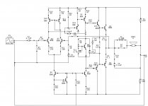
Going back to the original schematic....
I have built pretty much this circuit myself. I had 47 ohm resistors before the current mirror in the LTP, and the current sink was an LED-referenced one, but it worked OK.
Things to check:
1) LTP total current - should be around 2mA.
2) VAS current - should be 7-10mA
3) Power and signal grounds should NOT be mixed! This is the most important one especially with the CFP output stage.
I found 0.33 or 0.47 ohm collector resistors in the output stage just fine, despite what many here say.
The output inductor/resistor is a good idea, but in this case, the output zobel network works better if it is placed across the speaker terminals, i find.
Personally I feel the problems with this amp will be mostly down to PCB layout. The CFP is a bitch unless you lay it out well. I prefer Triple Darlington myself.
i can not understand why you used current source load for first stage, then shunt it with a 1Kohm resitor, doing so, you decreased the gain of the first stage and the use of the current source load then becomes questionable. maybe you are better off with just a resistor as load. C1 can be connected to base of Q3.
http://www.lh-electric.4t.com/gnd_loop.htm
http://aikenamps.com/StarGround.html
For general PCB design info, this is an excellent guide:
http://alternatezone.com/electronics/files/PCBDesignTutorialRevA.pdf
Basically, keep all the grounds that are to do with signal (the input filter stage grounds, the ground for the current sink, the VAS buffer ground, the feedback path ground) seperate from the grounds that join the power filter capacitors to ground. The best way is to have all these signal grounds meet at one point in a "star" shape, and then join this with one track, to the point where the pcb power ground connects. DONT return the speaker ground to this point either, return it to your power supply's ground point, at the capacitors.
I would show you an example of that on a PCB i've made but i'm away from home at the moment and don't have my PCB artwork on my laptop.
Biasing question
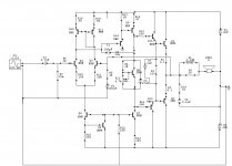
Thanks for the tips jaycee. I've built a prototype of the attached schematic and its working fine. I've tried to set the bias by measuring the voltage drop across R1 and R2 but i get no voltage on my meter. Is this normal or is there another way to set the bias e.g. an ameter in series with Q1?
Thanks for the tips jaycee. I've built a prototype of the attached schematic and its working fine. I've tried to set the bias by measuring the voltage drop across R1 and R2 but i get no voltage on my meter. Is this normal or is there another way to set the bias e.g. an ameter in series with Q1?
Attachments
- Status
- This old topic is closed. If you want to reopen this topic, contact a moderator using the "Report Post" button.