hey,
i was toying around with complimentary feedback pairs and i was wondering if ring of two constant current source was superior to a jfet ccs? i was thinkin of some run off the mill 2n5484s.
thanks a million!
i was toying around with complimentary feedback pairs and i was wondering if ring of two constant current source was superior to a jfet ccs? i was thinkin of some run off the mill 2n5484s.
thanks a million!
Although a simple JFET (or a depletion-mode MOSFET) CCS won't have as high an impedance as the ring-of-two at low frequencies, it will maintain its CCS behavoiur up to a higher frequency. This is because of the 'Miller' capacitance causing NFB that lowers the Z-out of the 'ring' circuit as the frequency increases.
Also the 'ring' circuit hac poor dc performance over temperature, as the current setting is determined by the Vbe of the bottom transistor.
I've seen people using 'ring' constant current loads for long-tailed-pair double-triode phase splitters in valve amps who wonder why the phase splitter performance is so poor at higher frequencies!
Attachments

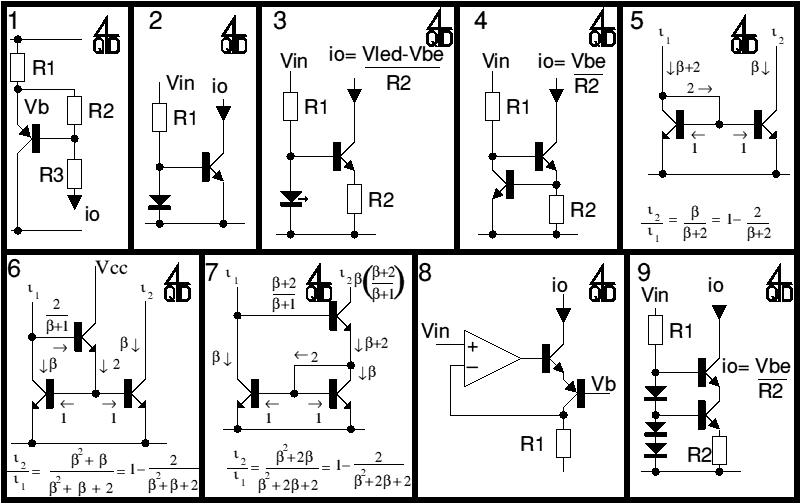
Anybody knows what constant current source that can work properly only under 0V3? In figures above all needs more than 2 diode/VBE drop to form CCS.
lumanauw said:Anybody knows what constant current source that can work properly only under 0V3?
In figures above all needs more than 2 diode/VBE drop to form CCS.
Current Mirrors can have drop lower than 0.2 Volt.
Say you want a low drop current source from negative rail.
To feed a dual NPN differential pair.
You then make a current source from POSITIVE rail
and under NPN pair, at negative rail,
you put a simple (two transistors) current mirror
to bias the differential pair.
To increase precision, if you need very good precise current source,
you might even use small value emitter resistors
in the two transistors in mirror.
Say with only 0.05-0.02 Volt volt drop at chosen current.
This will lower the saturation margin, Vce in mirror transistor (Vce 0.25-0.28, instead of Vce=0.30)
So, if you do not need absolute highest precision,
you should use a current mirror wthout emitter resistors.
To maximize Vce and avoid saturation in mirror transistor.
Hi, Lineup,
This is my problem 😀
I wanted to replace R3 (4k7) with CCS to give constant current benchmark for Q3 base.
I don't want to built current mirror between Q1 and Q2's collector, because current mirror there also gives non-constant current source for base of Q3 (Resistor at R3 also non-constant, depending the voltage drop accross R3).
The problem is because Q3 is bipolar. If Q3 is Vmosfet with drop 3V5, I can make transistor CCS based by 2x4148 or led as reference, because the margin is high. But if Q3 is bipolar without any RE, the margin is only 0V6.
Do you have reference, what CCS will fit in position R3? How do IC designers makes CCS inside opamp?
Attachments

The ring of two CCS is only better than a JFET if the reference transistors collector resistor is fed from an extremely stable voltage.
Cant you do as I said.
Make a constant current source coming from V+ (positive supply rail)
using two PNP transistors, or two diodes and one PNP with an emitter resistor.
This current is feeding a current mirror, using figure 5 in CCS and mirrors alternatives, in an earlier post above.
Current mirror is two NPN attached to negative rail.
With the mirrored current output connected to Q3 base.
I do not know if i can tell it more clearly.
lumanauw said:Hi, Lineup,
This is my problem 😀
I wanted to replace R3 (4k7) with CCS to give constant current benchmark for Q3 base.
I don't want to built current mirror between Q1 and Q2's collector, because current mirror there also gives non-constant current source for base of Q3 (Resistor at R3 also non-constant, depending the voltage drop accross R3).
Ah, yes - but not if you put a capacitor between the mirror common base and emitter (or power rail, if you use emitter degeneration). This way, the mirror works as a mirror only for low frequencies, which is advantageous to keep the LTP currents at DC balance. However, for AC, there is constant, thermaly compensated (by the paired transistor in the mirror) voltage on the base, reducing the mirror to a current source working at 1/2 the tail current.
The problem is because Q3 is bipolar. If Q3 is Vmosfet with drop 3V5, I can make transistor CCS based by 2x4148 or led as reference, because the margin is high. But if Q3 is bipolar without any RE, the margin is only 0V6.
The question is, why does this current need to be constant? Granted, a current mirror instead of R3, that mirrors the other leg of the LTP could be considered a push-pull drive for Q3. Are you trying to insure it works in class A, or something like that?
Do you have reference, what CCS will fit in position R3? How do IC designers makes CCS inside opamp?
Usually by feeding a multiple current mirror with a reference current generated by a different current source. You could use the same approach, but the way I outlined above gives better results (it's self-adjusting) and uses less parts (5 maximum).
BTW the schematic you have posted has some serious problems. It has been stripped of all components bar the ones that insure VERY basic functionality.
1) Q3 is very underdimensioned for it's job. It will be very hot even for low rail voltages, and more than +-30V would be asking for serious trouble. I would use something that can be attached to a heatsink instead.
Look for a transistor with high hfe and Ft here. A BD 139 selected for highish hfe should do fine for starters. I would not operate that amplifier without this mod!!!
2) The bias is VERY inadequate. It puts the amp into class B (in fact, the bias voltage is below the drop in the Vbes of the transistors, you could call it class C). It is clearly designed to produce sound, without blowing itself up - and that wouldbe the end of it. It will sound rather bad at low outputs! A proper Vbe multiplier would do the trick, at the expense of one transistor, two resistors and a trim-pot. It would also be nice to bypass it with a capacitor.
3) R6 as a pull-up for the VAS is a rather bad idea. Slew rate will be asymetric, and so will the clipping. Also, more odd harmonic distortion would be generated. The simple solution would be to make it into a bootstrap arrangement. To do this, split the 2.2k resistor into two equal series connected parts, say 1k or 1.2k. Connect capacitor (it will probably need to be electrolytic) with + to the 'middle' between the two resistors, and - to the output of the amp.
Once these mods are done, only then you can expect any real difference from your 'CCS' modification. The above mods would be in order of priority - for instance, if you use the bootstrap mod, and don't correct the bad biassing scheme first, the result willa ctually be WORSE.
4) Finally, you might want to filter the positive rail for the LTP, this is not a major issue but also relatively easy to do. Add the same value resistor as you used to split R6 for the bootstrap (so 1k or 1.2k) in series with the 47k tail, closer to the power rail. Then connect the joining point of this 1k and 47k to + of a capacitor, and the - of this capacitor to ground. Make the capacitor the same as the bootstrap capacitor. This should give you some rough minimization of the 'thump' in the speaker when powering up the amplifier.
Hi, Lineup,
I get your idea 😀 Something I wanted to ask. In fig5, consider the emitors are sitting at 0VDC. The base will be at 0V6. The left collector will be also at 0V6, it is connected to common base.
Hi, Ilimzn,
Thanks for your explenation. I wanted to tell you first, the schematic attached above is from another thread "Peace". I used it here, because it has exactly the same Q1, Q2, Q3, R3 that fits my question.
I imagine silly things 😀 Maybe it is rare that people matters this. Resistor for R3 position is already taken as "it is suppose to be there" from before I even born until today 😀 In configuration of Q3 like that (no RE), maybe 20mV d-VBE has already swing the output fully from +rail to -rail.
But let's pretend we have "a very low gain transistor" at Q3. It needs input from 0V-VBE to 0V6-VBE to make full swing from -rail to +rail.
Q1 collector can give current, but cannot suck current from Q3's base. The only thing that can suck Q3 base is R3. If this "low gain transistor" base is at 0V6 (towards -rail), then the current sucked by this 4k7 is 0.128mA.
If the voltage at this 4k7 is only 0V3, the current sucked is only 0.064mA. This current will go lower and lower and lower depending the voltage drop at 4k7. The suck out action by R3 is not constant. This is what I wanted to encounter. So, if Q1 is not working it's job, "something" in R3 position must be sucking current, but in constant mode, not like I=V/R.
I think replacing R3 with "somekind of CCS" that can work fine below 0V6 will give much lower THD 😀
I get your idea 😀 Something I wanted to ask. In fig5, consider the emitors are sitting at 0VDC. The base will be at 0V6. The left collector will be also at 0V6, it is connected to common base.
Is it OK for the right transistor if it's collector is under 0V6 (collector voltage is lower than base voltage)? You said the lower saturation margin is 0V3. This is the "margin", maybe the right transistor don't work very well at collector sitting at 0V3? Or it is not a problem, it works well also at 0V3 collector voltage?This will lower the saturation margin, Vce in mirror transistor (Vce 0.25-0.28, instead of Vce=0.30)
Hi, Ilimzn,
Thanks for your explenation. I wanted to tell you first, the schematic attached above is from another thread "Peace". I used it here, because it has exactly the same Q1, Q2, Q3, R3 that fits my question.
What is the value of capacitor needed? In values of nF or uF?Ah, yes - but not if you put a capacitor between the mirror common base and emitter (or power rail, if you use emitter degeneration).
I know this question will arise sooner or later 😀The question is, why does this current need to be constant?
I imagine silly things 😀 Maybe it is rare that people matters this. Resistor for R3 position is already taken as "it is suppose to be there" from before I even born until today 😀 In configuration of Q3 like that (no RE), maybe 20mV d-VBE has already swing the output fully from +rail to -rail.
But let's pretend we have "a very low gain transistor" at Q3. It needs input from 0V-VBE to 0V6-VBE to make full swing from -rail to +rail.
Q1 collector can give current, but cannot suck current from Q3's base. The only thing that can suck Q3 base is R3. If this "low gain transistor" base is at 0V6 (towards -rail), then the current sucked by this 4k7 is 0.128mA.
If the voltage at this 4k7 is only 0V3, the current sucked is only 0.064mA. This current will go lower and lower and lower depending the voltage drop at 4k7. The suck out action by R3 is not constant. This is what I wanted to encounter. So, if Q1 is not working it's job, "something" in R3 position must be sucking current, but in constant mode, not like I=V/R.
I think replacing R3 with "somekind of CCS" that can work fine below 0V6 will give much lower THD 😀
I think is a godd idea, change the biasing for a CSS! This 1n4148 isn't good for HiFi aplications!
lumanauw said:Is it OK for the right transistor if it's collector is under 0V6 (collector voltage is lower than base voltage)? You said the lower saturation margin is 0V3. This is the "margin", maybe the right transistor don't work very well at collector sitting at 0V3? Or it is not a problem, it works well also at 0V3 collector voltage?
This depends on the transistor saturation characteristic, but usually for low currents like one would use in a LTP, this will be well below 0.3V.
Hi, Ilimzn,
Thanks for your explenation. I wanted to tell you first, the schematic attached above is from another thread "Peace". I used it here, because it has exactly the same Q1, Q2, Q3, R3 that fits my question.
What is the value of capacitor needed? In values of nF or uF?
It could probably be calculated from the dynamic resistance of the base given LTP current and hfe of 'current mirror' transistors. It still comes out in the uF region I think, but for your purposes this may not be a problem. You really need that current mirror to become a current source at HF so some positive effect would happen already in the tens of nF region. 47uF would bring it to well below 20Hz.
I know this question will arise sooner or later 😀
I imagine silly things 😀 Maybe it is rare that people matters this. Resistor for R3 position is already taken as "it is suppose to be there" from before I even born until today 😀 In configuration of Q3 like that (no RE), maybe 20mV d-VBE has already swing the output fully from +rail to -rail.
But let's pretend we have "a very low gain transistor" at Q3. It needs input from 0V-VBE to 0V6-VBE to make full swing from -rail to +rail.
Q1 collector can give current, but cannot suck current from Q3's base. The only thing that can suck Q3 base is R3. If this "low gain transistor" base is at 0V6 (towards -rail), then the current sucked by this 4k7 is 0.128mA.
If the voltage at this 4k7 is only 0V3, the current sucked is only 0.064mA. This current will go lower and lower and lower depending the voltage drop at 4k7. The suck out action by R3 is not constant. This is what I wanted to encounter. So, if Q1 is not working it's job, "something" in R3 position must be sucking current, but in constant mode, not like I=V/R.
I think replacing R3 with "somekind of CCS" that can work fine below 0V6 will give much lower THD 😀
Well, actually, a current mirror is what is used for precisely the reason you mention. Otherwise, in order to speed up Q3, the base current needs to be much smaller than the LTP tail current / 2, AT ALL TIMES - difficult because you also want the tail current to be just slightly above base current at Q3 saturation, otherwise you get charge storage efects ('sticking' to the rail as the amp goes out of clipping).
With current mirror, the base current maximum becomes + or - tail current of the LTP. With current mirror that degenerates into current source, it becomes + or - tail current /2 but HF performance may be better. Either way, charge 'suckout' is improved. Things can be further improved by not alowing Q3 to go into deep saturation, this you can do by adding a clamping diode arrangement around Q3.
Although your reasing is sound, a standard current source is not a good thing to use, because it's 'value' would be very difficult to establish. Ideally, it would be tail current /2 minus base current of Q3, but base current of Q3 is not easy to define and depends on many factors (keep in mind that Q3 gain is variable with many parameters). You could use an approximate value, but then any imbalance throws your LTP out of symetry. This may, however, be what you want - even level distortion will increase (possibly quite substantially), beyond what the simple resistor would produce. The 'degenerated current mirror' approach, however, 'automatically' tries to keep the balance, without the need to adjust a separate current source in proportion with LTP tail current.
Hi, Ilimzn,
Yes, at first sight putting current mirror at Q1-Q2's collector seems the same as my intention. But it is different. Mirrored ccs by right leg differential is not constant at all. Putting current mirror between Q1-Q2's collector makes the gain doubles, but not lower the distortion caused by Q3 base (non constant charge suckout at Q3's base)
Transistor is not good at 2 things. Fluctuating voltage and fluctuating current. In VAS collector, some people cascode the output collector to minimize fluctuating voltage (early effect). I'm trying to experiment with fluctuating current here.
In position of R3, the non-constant current (because of relation I=V/R) is worsen to the final result, because this non-constant suck out is directly feeded to base (Q3's). As a result, distortion by non linear base suck-out is magnified by Q3 itself.
I need CCS that is constant all the time (not induced by opposite collector, like in current mirror) to gain my goal.
Try this. In my experiment it gives far better sonic, less high order intermodulation, so my conclusion CCS in position R3 should be a stiff-stand still one.
Like you said, the value of this R3 CCS should be 1/2 of tail current fed the differential pair.
In left drawing it is the standard configuration. R1 is 680ohm, feeded from +30V. The right drawing gives better sonics. R2 is valued 30Kohm and feeded from extra rail +60VDC. In right figure, the current suck out by R2 is relatively constant (compared to left drawing). Putting CCS there should be better 😀
But making additional rail voltage is not practical 😀 I wanted somekind of CCS in postion of R3, feeded from the same power rail.
Attachments

Your picture on the right would have been my first recomendation save for teh fact that the auxiliary power is usually impractical.
It sould be noted that base suckout is not a constant even with a CCS because in a real application there is feedback via LTP to the base of Q3. Because of this, you can only guarantee constant current when the feedback is not working, i.e. at some sort of clipping situation. During this situation, the difference between a CCS and a current mirror is only in the magnitude of the current. The charging or discharging is constant. The resistor situation suffers from the 'inverse exponent' law that slows down the speed of suckout as it progresses, and in this I understand your point.
What I am trying to say is that a CCS solution is the right one in theroy, but is difficult to properly implement. This is because, in order to keep the input LTP in balance (and minimize it's nonlinearity, see D. Self's site for this), you need EXACTLY 1/2 of the LTP tail current +- the tolerance between the LTP transistors, which will, for reasonably high hfe, be very tight. In other words, you need two separate CCS, with very tight tolerances (or adjustable) but also, with good thermal tracking. It should be noted that misadjustment of the tail current to your CCS current ratio will have a MUCH more profound impact on sonics than the change from resistor to CCS because of changed balance of the LTP and therefore changed nature of it's nonlinearity.
Because of this problem, I proposed a current mirror that is prevented from mirroring anything but very low frequencies ('near DC'). Such a current mirror willa tomatically attempt to establish LTP balance, therefore solving your adjustment problem. By varying the degeneration resistors in the mirror you could even deliberately introduce LTP unbalance for a desired sonic effect. However, for audio AC signal, this current mirror is prevented from 'mirroring' the other LTP leg, and reduces to a current source at the place of R3, with pretty much exact and automatic setting to LTP tail current /2, without low tolerance components or adjustment. A minimum of degeneration in the emitters of the LTP and current mirror, plus relatively close mounting of LTP and mirror transistors will also insure good thermal tracking.
Hi, Ilimzn,
Thanks for the explenation. I will try current mirror+capacitor like your suggestion. The right drawing (with 60V rail) really sounds better in real amp 😀
Thanks for the explenation. I will try current mirror+capacitor like your suggestion. The right drawing (with 60V rail) really sounds better in real amp 😀
It would be worth investigating why. The value of the constant current is important, or more appropriately said, it's ratio with the tail current of the LTP.
That being said, the exact nature of drive for Q3 lessens in importance the smaller it's base current is compared to the leg current of the LTP (so you can influence this by using larger LTP tail currents, or higher gain for Q3) - this is another variable you may want to invetigate.
You could also try a regular current mirror, but delibeeately imbalance the LTP by changeing the degeneration resistors in the mirror (their ratio corresponds to current ratio in the mirror).
- Status
- Not open for further replies.
- Home
- Amplifiers
- Solid State
- constant current source