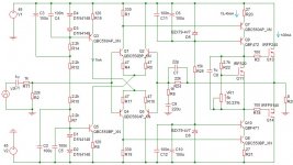
Hi. This is my finall design, so does anyone has any proposition before i start to build it?
1. I raised diff. stage current to 3.5mA per device, the higher idle current, better slew rate, isn`t that right?
So why in all classic designes, the diff.pair idle current`s 500uA to 1.5mA max??? The devices I`m gonna use (BC550) in this case could go even higher than 3.5mA...
2. Where should I connect hf compensation capacitors in vas stage Q9/Q10 base-emmiter?
3. The idle current of output mosfets is set to 100mA any suggestions?
4. Does anyone have spice model for BF872, I`d like to use them in vas stage instead BF471/472.
THank you ALL in advance!
Attachments
bogdan_borko
1.
I also prefer using more current in input stage.
Somwhere between 2-5 mA in each transistor.
Sometimes this can create DC-offset problems, as there is higher input bias current.
But in your case, with 2 symmetrical diff input pairs
and the use of C9 - DC-blocking capacitor in feedback
this will be no problem.
In fact, you maybe even will be able to remove C9 without any offset problem.
4.
As far as I know, BF471/472 is very much the same as BF871/872.
They are used as cascodes in your circuit,
so I think any simulation result will be just the same.
Here is a Philips spice model of BF871:
http://www-us.semiconductors.philips.com/pip/BF871.html
I leave the rest of questions for other to answer.
Finally, I think you have learned a lot and your circuit looks very good, to me!
Good working, bogdan_borko!
Hi Bogdan,
Stick with BF471/472, they will performe excelent in your circuit, lose cascode Q7/8 with BC550/560, they cannot withstand 15mA without trouble, or convert circuit into folded cascode with new biasing aragement (similar to yours), put RF blocking cap in parallel with R2 like 100p, put trimer in one of diff. pair to control DC offset or include servo that will control current betwen R10/12.
Ciao, a
bogdan_borko said:Hi. This is my finall design, so does anyone has any proposition before i start to build it?
What about , a bipolar driver for driving the output Mosfets, they help to isolate the non linear input capacitance of the mosfets , from the high output impedance , cascode VAS...
Ah...and a zobel at the output (10 Ohms- 100 nF )...
Hi bogdan,
If the transistors (Q1,2,4 and 6) are all matched for gain, and the current sources are equal, the higher emitter current should not cause DC offset issues at all. Thermally couple them.
You might want another set of outputs for reliability. Prototype it and see how it behaves.
-Chris
If the transistors (Q1,2,4 and 6) are all matched for gain, and the current sources are equal, the higher emitter current should not cause DC offset issues at all. Thermally couple them.
You might want another set of outputs for reliability. Prototype it and see how it behaves.
-Chris
bogdan_borko said:is there eny other bc transistor with lower noise then bc550/560?
No!
BC550C and BC560C is as low noise as you can get.
I always use C version, because they have highest gain.
bogdan_borko said:Hi. This is my finall design, so does anyone has any proposition before i start to build it?
1. I raised diff. stage current to 3.5mA per device, the higher idle current, better slew rate, isn`t that right?
Yes.
Importantly, the gain increases as well, but you can trade tht for improved linearity by increasing the emitter resistors. There is, however, a compromise involved - with noise. This should not be a problem as you are designing a power amp so inputs signals are relativeli high and gain is not extreme.
The relationship between tail current and noise is not simple, there is usually a minimum, lower and higehr currents will increase it (but different mechanisms are involved). Input degeneration may also increase noise - however, as I said, in your case it should not be a problem - while the added linearity is a worthwhile goal.
Keep in mind ALL your stage currents are dictated to some extent by the LTP tail currents. This means that you want to make these thermally stable, at the moment they have a negative tempco, so as temperature increases, they decrease. Fortunately, in your amp this should not be a serious problem. Of course, R10 and R12 could have been a single resistor
So why in all classic designes, the diff.pair idle current`s 500uA to 1.5mA max??? The devices I`m gonna use (BC550) in this case could go even higher than 3.5mA...
See above about noise.
You should also keep in mind that you cannot directly compare single and complementary diff inputs. as well as tail CCS topology and tail resistor topology. Increasing tail current for asymetric diff stages increases input bias current, which also increases DC offset. Wit symetric complementary diff. inputs the bias current is largely compensated, so higher tail currents can be used for equal DC offsets. There are other repercussions to do with differential input impedance of a LTP, which comes into play at HF - increased tail current decreases it.
Finally, there is the issue of power dissipation - typically an input transistor in a simple non-cascoded LTP has to span one whole supply rail across C-E, and this multiplies with the tail current/2.
2. Where should I connect hf compensation capacitors in vas stage Q9/Q10 base-emmiter?
Q9 collector to Q7 base, similar for the other side...
3. The idle current of output mosfets is set to 100mA any suggestions?
Should be fine...
You need gate protection zeners. Alternatively, although not immediately obvious, a reverse polarized diode from G to S of bothe MOSFETs will imit the gate voltage to the bias voltage plus 0.7V, but as this will typically be about 6-7V, the current limit will end up too high. Keep in mind you need to check Vgs versus Id plots for higher temperatures when choosing current limiting zeners!
4. Does anyone have spice model for BF872, I`d like to use them in vas stage instead BF471/472.
THank you ALL in advance!
These are not terribly critical, as they work in a cascode configuration as the common base part. As such their gain will be maximized and bandwidth practically solely dependant on the effective capacitance they see to ground, in this case the overwhelming contribution will be the output MOSFETs - BJT Cob will be negligible for any half decent transistor, in comparison. In theory, what limits you here is the current at your disposal, as this is what will be charging and discharging these capacitances. The current gain is provided solely by the common emitter devices, in your case BC550, 560.
Aparatusonitus mentions that these will not withstand 15mA, which is completely incorrect - since the C-E voltage is limited by the cascode arrangement, these can be run at quite high currents, and their gain exploited to the max. There are, however, concerns as to the design of a cascode driver, which I will address in a moment.
You could probably use BD140/139 (assuming C-E max voltage is within limits) without any great consequence to the performance here. What does count, is how well the chosen BJTs can dissipate power (as well as other SOA requirements).
With a cascode output stage, there are some points that need to be addressed:
1) Output impedance is very high, and voltage gain depends almost exclusively on the output impedance. This can present a problem as the output impedance, in your case, are the output MOSFETs. Although their input capacitance nonlinearities are somewhat compensated, for larger signals (as Vds becomes low), the nonlinearity directly impacts OL gain. Two approaches used to counter this are a) a buffer stage, and b) a stable shunt impedance to 'swamp out' the next stage nonlinear impedance effects (this, in your case, would be a resistor from driver Cs to ground). The first adds one stage and associated problems, the second reduces OL gain (not necesairly a problem). A combination can be used as one tends to partially cancel out the other.
2) You lose output swing, the output can only swing as far as Vrail minus cascode voltage. So, you want the cascode transistor base to be fairly close to the rail, keeping in mind the C-E voltage of the current gain BJT des to some extent impact it's gain. Since there tends to be rail droop as the power increases (i.e. output is required to swing closer to the rails), in many cases a 'halfwave rectifier' is added between the rail for the output MOSFETs and the driver side of the amp, in order to extend the maximum output swing. If properly constructed, this also filters out a lot of the halfwave-rectified-output-current artifacts created in the output stage, from being egenerated into the input stage via the rails.
3) Consider what happens when this amp clips. In theory, the full LTP tail lcurrent is available to drive the lower transistors in driver cascodes. Using the typical configuration and beta of these devices, we end up at cascode currents on the order of amperes, if the current is not limited. Fortunately, you have included Re's on the lower BJTs, so current is limited to 63mA, and maximum voltage between base and power rail is about 2.3V (LTP tail urrent times 330 ohms). The cascode voltage should not be lower than this, so there we have another compromise.
All in all, I think you have done very well! Just put the output MOSFETs on a very god heatsink and mount them properly for minimum thermal resistance - or, even better, you may consider powering the MOSFETs from a separate power supply with lower rail voltages.
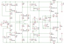
ok, this is the update...
I limited the current to ~47mA, and connected the diodes between the output and vas stage(I hope I understood it well)?
1. THe firs thing I didnt understand, is where to put resistors for stable shunt impedance? collectors of Q9 and Q10 to the ground? What should be the value of these resistors?
I limited the current to ~47mA, and connected the diodes between the output and vas stage(I hope I understood it well)?
1. THe firs thing I didnt understand, is where to put resistors for stable shunt impedance? collectors of Q9 and Q10 to the ground? What should be the value of these resistors?
Attachments
The resistors to reduce Open Loop gain
is from Q9 collector to ground and other from Q10 to ground.
Value can be something like 10k - 22k.
If we look at Q7, the emitter resistor is 100 Ohm.
The gain in Q7 then is reduced to 10k / 100 = 100
or 22k / 100 = 220.
As the gain is mostly determined by 10k ( or 22k ) resistors,
this gives better linearity. ( Resistor is very linear load compared to transistor, MOSFET Gates )
===================================
The gain in input stage transistors is:
680 / 47 Ohm ~ 15
The total open loop gain will be = gain in input stage x gain in VAS stage.
The feedback will be = Open Loop Gain / closed loop gain.
You have closed loop gain (22k/1k) + 1= 23
Say open loop gain is 2300, this gives a feeback factor of:
2300 / 23 = 100
So the amount of feedback will be 100 = 40dB
40 dB is a normal feedback.
===================================
You can put in compensation caps, as told between Q7 base and Q9 collector ( and Q8 base to Q10 collector )
Maybe a good value to start with could be 47 pF caps.
===================================
As mentioned, you will probably not have much problem with DC-offset.
Especially if your input stage have transistor pairs that are closely matched.
You could probably removed C9 and C14.
I do not think you will get much DC-offset, if you do.
bogdan_borko said:ok, this is the update...
I limited the current to ~47mA, and connected the diodes between the output and vas stage(I hope I understood it well)?
Yes... but you need two large capacitors on the other sides of the diodes (the driver side). These will hold the local rail voltage high when the actual rail droops under load.
Current limit of the driver stage was ok even at 63mA, you are still (although barely) under the BC550/560 SOA, but this sort of current will only be demanded from the amp under extraordinary conditions, not in normal operation.
You still miss MOSFET gate protection diodes. As it is now, even a momentary short on the output, normally easily survived by the MOSFETs if fuses are included in the drains, will kill them instantly, even with the fuses. This is because Vgs will momentairly go to almost the full rail voltage, which is higher than the maximum +-20V. Current limit is secondary here - any break of NFB operation for any reason (oscillation, very reactive load, short), will result in the driver stage attempting to drive the MOSFET gates as far as they will go - which is essentially rail voltage minus 4.7V. Omitting these diodes is a classical beginner's mistake which tends to fry the MOSFETs for 'unknown reasons' (trust me, this is from bitter experience
). Do not confuse VMOS with LMOS, most if not all LMOS have built in gate protection, VMOS do NOT!1. THe firs thing I didnt understand, is where to put resistors for stable shunt impedance? collectors of Q9 and Q10 to the ground? What should be the value of these resistors?
Lineup has already provided a good explanation...
BTW I would not recomend a 4 ohm load unless your power supply was deliberately made 'soft' but that has other unwanted repercussions. You may get away with it if you use two isolated heatsinks (so no mica is needed between MOSFET and heatsink), and also remove the anodization where the transistor is in contact with the heatsink - which needs to be VERY big. Alternatively, you could solder the transistors onto a copper heat spreader, then mount that isolated onto a heatsink. In both cases you need premium thermal greese. Neither of these options is trivial, the idea is to have minimum thermal resistance. One pair will, however, work fine with an 8 ohm nominal (4 ohm minimum) load.
My sincerest recomendation would be to use a lower voltage power supply for the output MOSFETs. Your driver stage plus MOSFET Vgs at maximum current already loses about 8-10V off each rail, on the MOSFETs, and this is simplu just heat - not something you want here. Using 35V rails for the output would probably make very little difference in performance, but would quite signifficantly reduce dissipation on the MOSFETs, i.e. alow you the use of lower load impedance with a given heatsink.
There is always the possibility of paralleling output devices, but I have found that the elimination of the source resistors that is possible when a single pair is used, has some sonic advantages - even if it means a lower output power.
Oh, and BTW, I am HARDLY 'almighty'
bogdan_borko said:is there eny other bc transistor with lower noise then bc550/560?
Although it's not BC, how about the KST5089 from Fairchild? This one is only 25V instead of 30V, but also has a fairly linear Hfe of around 600!
http://www.datasheetarchive.com/semiconductors/pdfdatasheet.php?Datasheet=1078145
I suppose it could be complemented with KST5087.
ilimzn said:I am HARDLY 'almighty'
No, but you are good.
Attachments
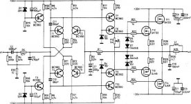
jacco vermeulen said:No, but you are good.
Regarding comp caps, see also previous posts by ilimzn and me.
In jacco v attached symmetrical input MOSFET output amplifier
68pF compensation caps is put in input stage.
This might be an alternative to try.
This amplifier is very similiar to bogdan_borko amp.
Uses fully symmertical BC550/560 input biased with CCS, Constant Current Sources.
Cascoded VAS and MOSFET push-pull output.
To use separate supplies, for input/VAS and output,
in this case +24 Volt and +20 Volt, is a very good option.
Hi bogdan, i have also some comments about your amp...
Maybe you should reduce powersupply a bit (36v ?), bc550/560 has max rating of 45v, including swings from inputsignal and variations from powersupply you risk blowing the inputstage.
You should also observe dissipation in Q3/5, 7ma*45v=315mw, they might be too hot to touch. An inputfilter is always helpful, maybe a 100pf in paralell to R2 ? You should use basestoppers for Q9/10, it's very likely they enter parasitic oscillation without them. (~47-150ohms).
15ma in vas might not be enough to drive the mosfets for higher frequencies ?
R7/10/12/14 will need to be 2watt versions, you have 225mw dissipation here. The same for r25.
Mike
MikeB said:Hi bogdan, i have also some comments about your amp...
Maybe you should reduce powersupply a bit (36v ?), bc550/560 has max rating of 45v, including swings from inputsignal and variations from powersupply you risk blowing the inputstage.
Well spotted, MikeB, see, you are far more mighty than I am
At one time I did have a similar problem, I just solved it by including zener clamps to the LTP common emitter points, rarther than going to cascode, or using different LP transistors. However, I also had a regulated power supply for the front end... more below.
You should also observe dissipation in Q3/5, 7ma*45v=315mw, they might be too hot to touch.
This is one reason why I mentioned a higher reference voltage for the CCS, which means higher Re's for the CCS transistors, and also lower Vce for them, therefore lower dissipation. Also, the CCS thermal dependence may be lower. Since the reference is bypassed heavily, normal zener diodes would work here, 24V say.
Alternatively, you can use a series resistor between the CCS and the LTP tail, to drop voltage and take over some power dissipation. My favorite way of doing this is actually providing two separate resistors twice the value, one to each LTP emitter. Then, the emitters are connected with a single resistor. This alowes the use of lower power resistors as there are two to dissipate the heat, and also adjusts LTP degeneration using a single resistor - while keeping the number of components the same. The circuit is actually a star-to-triangle transformation from the classical 'separate emitter resistors + voltage drop resistor' topology. For the voltage drop resistor >> emitter resistors, this is easy to approximate by using the E-to-E resistor as 2x previous Re, and splitting the voltage drop resistor into equal parallel resistors twice the value.
The 24V CCS reference version has an advantage if you ever want to cascode the LTPs (to be able to use low Vce low noise parts safely), since you can use the opposite references as the cascode transistor base voltage.
15ma in vas might not be enough to drive the mosfets for higher frequencies ?
It should be just fine for a single pair, remember that you are essentially only driving a bit more than the Cgd of both MOSFETs (Cgs are bootstrapped by MOSFET follower action).
Yes, the series resistor in the ccs to ltp is the easiest way out... In this case i would still prefer the 2bjt-ccs, it's thermal completely stable. (the sensing bjt sees practically no dissipation (Vce=1.2v), and will reduce current when heating up).
About the ltp-devices, 2sc2240/sa970 might be a way out ?
Mike
About the ltp-devices, 2sc2240/sa970 might be a way out ?
Mike
- Status
- This old topic is closed. If you want to reopen this topic, contact a moderator using the "Report Post" button.
- Home
- Amplifiers
- Solid State
- Question for all mighty ILIMZN and others...