MikeB said:Yes, the series resistor in the ccs to ltp is the easiest way out... In this case i would still prefer the 2bjt-ccs, it's thermal completely stable.
I have to admit I am not a big fan of those as I had some rather nasty experiences with oscillation. Also, these ar e not inherently thermally stable because the sensing BJT d(Vbe) is still not compensated - while the CCS d(Vbe) is invisible through the feedback action of the sensing BJT. Trust me, I used this fact for a bias servo on an experimental amp
") On the other hand, a 6V1 zener plus diode in series tend to compensate the BJT in a standard CCS arrangement very well, how well depends on the zener current chosen. This can be somewhat of a problem as the 'ideal' value depends on the actual construction of the zener, it varies somewhat from manufacturer to manufacturer and type to type, even for the same 'ideal' voltage (5-6V). However, in this amp this is not a great problem,a s there is no thermal feedbac and no chance of runaway, also, MOSFETs are FAR less critical as to the idle current chosen, so a +-10% variation with temperature and rail voltage is no tragedy by far.
On the other hand, a 6V1 zener plus diode in series tend to compensate the BJT in a standard CCS arrangement very well, how well depends on the zener current chosen. This can be somewhat of a problem as the 'ideal' value depends on the actual construction of the zener, it varies somewhat from manufacturer to manufacturer and type to type, even for the same 'ideal' voltage (5-6V). However, in this amp this is not a great problem,a s there is no thermal feedbac and no chance of runaway, also, MOSFETs are FAR less critical as to the idle current chosen, so a +-10% variation with temperature and rail voltage is no tragedy by far.Yes, my idea was that the sensing BJT does not heat up, at least not by it's own dissipation. As it only measures the current through the RE of the other bjt, the vbe change of that has no real effect. And if the sensing one heats up, the current supplied by the 2bjt-ccs drops and does not increase...
But, that's not what the threadstarter was interested in...
Mike
But, that's not what the threadstarter was interested in...
Mike
ilimzn said:
Yes... but you need two large capacitors on the other sides of the diodes (the driver side). These will hold the local rail voltage high when the actual rail droops under load.
How about reactive loads?
Cheers Michael
Ultima Thule said:
How about reactive loads?
Cheers Michael
Works either way. The benefit is solely dependant on rail droop and transformer regulation, of course, both will be taxed extra for reactive loads.
Have a look at the waveform of an amp power rail working at high power into a load, and you will see a reverse sawtooth as the rectifiers charge the filter caps, and the amp discharges them. If you could zoom in, especially on the falling slope, you would see that it is a series of drops that occur as the output signal goes through the half period with the same polarity as that rail. This becomes very obvious if the amp is delivering output at a low frequency.
The idea behind the diodes is to 'catch' the top of the sawtooth into the local filter caps of the driver stage, the ones 'after' the diodes. This can also be done by providing a separate small bridge rectifier from the transformer windings, and separate filters (so in essence a whole separate power supply) for the driver stage.
Since your amp cannot swing over the top of the sawtooth anyway, the fact that you lose voltage to transformer regulation under load, is not a big problem. But, what the local rectifier gives you, is a supply voltage for the driver stage that is always close to the peak output of the transofrmer.
Since the amp loses about 8-10V off the rail voltage, without the extra I proposed, the amp always clips 8-10V below whatever the power supply is, including the sawtooth rail droop. This will be quite audible because the 100Hz sawtooth waveform intermodulates with the output, it will be VERY audible for low notes that are closer to 100Hz. This is disregarding anny effect of this power rail hash being regenerated into the amp due to limited PSRR.
With the addition I proposed, since the driver stage stays supplied with a voltage close to the peak of the rail voltage waveform, even when the actual rail for the output stage droops 8-10V, there will still be no clipping, because the cliping limit for the driver stage does not move with the rail droop.
How signifficant is this?
Let's assume a cascode + Vgs loss of this amp equals 10V, shich is a good worst case approximation. Let's also assume that under full load the top of the sawtooth on the power rail will drop to 40V due to transformer regulation, and the bottom will drop to 32V due to the filter caps used. Also, let's assume that the driver stage clips cleanly. All are actually quite reasonable assumptions, and the values are typical, maybe even on the pessimistic side.
For reference, let's use a case where the power rails are at 40V and ideally stiff. Due to the cascode + Vgs rail loss, the maximum output voltage will be 30V peak, and the power into a 4 ohm resistor would equal 112.5W at the edge of clipping. Also, clipping will be clean.
Without the proposed addition, the driver stage output voltage limit moves with the power rail sawtooth (for the moment we will disregard PSRR issues this creates). In order to be safe, you would have to lower the maximum output voltage by the size of the 'dip' in the swatooth, 8V. In reality, this will be less, because a lower output voltage will mean lower output current and a smaller dip - let's say 6V. The maximum output voltage is therefore 24V peak, the power into the same load will drop to about 72W, and what is worse, clipping will be very dirty with the power rail sawtooth imposed as the clipping limit, resulting in some rather nasty intermodulation. And, if your driver stages have PSRR issues, you will hear them!
With the proposed addition, the 8V dip in the power rail of the output stage is still less than cascode+Vgs losses, so aside from MUCH less intermodulation as Cgd is modulated due to varying Vgd, the maximum output voltage remains the same as for the stiff rail example, at 30V, so power at clipping limit is still 112.5W and clipping remains clean. This will be true as long as the rail droop from top to bottom of the sawtooth, remains below the cascode + Vgs loss.
And, you get extra benefits from the power rails of the driver stage being additionally filtered due to local filter caps after the diodes.
It appears to me that the 2 diodes and 2 caps extra per channel (or better still a separate bridge and two caps for multiple channels, since the current drain of the driver stage is low) are well worth the benefit.
Finally, let me remind you that you cannot combat rail droop by unreasonably increasing the number of microfarads of your main filter caps - when this is done, rail droop decreases, but only to a point - other problems crop in: diode peak current rises and with it you can get into nasty reverse recovery problems, plus you can drive your transformer core into saturation, which increases heat generation in the transformer very rapidly, as well as produces extra 100Hz electric, and (with saturation) magnetic hash - all the while, PSRR issues may only get better by 10dB. With the proposed modification, you relax the power supply requirements while simultaneously recovering some cascode+Vgs rail loss, and having this same loss act as a clean clipping limit, and you make PSRR issues much less of a problem as a 'free bonus'.
BTW why not simply re-use the cascode transistor Vb source (zeners) as the current source reference for your CCSs? You save yourself a number of components that way and reduce the Vce on the CCS transistors (right now they are working over the limit for any input voltage larger than zero ).
).HAllo everybody I`ve been on the job yesterday (whole day), so I couldn`t answer.
I`m working in hydro-power-plant(hidroelektrana-jebi ga kako se kaze...). (Maybe some milliapere that your aplifier`s eating right now, is made by me
1. Omitting gate diodes is not a mistake, that`s
alluding..(to se podrazumeva ako se tako kaze na engleskom)...
2. This amp is ment to work with 8 Ohm speakers (I used 4Ohms for simulation) In my mind if I make a simulation working good with 4 Ohms, then 8 Ohms should be less painful.. (theoreticlly) When I start to bild it , then it`s another question...
3. I already thought about that (lower rail voltage for fets) when i was buing my thorus tranformers, so I`ll do it (+/-40V-regulated for the driver stage and +/36V for the power stage)
4. In the meantime , your idea for the same voltage reference for LTP and cascode, crossed my mind too , so this is the finall update (I hope so). Lowering the driver stage voltage to 40Volts and css with zener diode refrence will solve the previus problems. Also when I do something, I do it right or i don`t do it at all, so I decided to do reguleted power supply for the driver stage, just one question about that: I hope the classic regulation circuit with zener diode and bjt will do the thing... ?
Thank you all !!!
Attachments

You really should add basestoppers to q9/q10, in case of clipping these will enter reversebias and suck down the voltage supplied by the zeners, then shutting down the ltp on the reverse side. This results in complete breakdown during clipping, it's even possible that amp stays flipped and needs to be "restarted" by shut down. (I already had that problem, destroyed a speaker...)
Also you risk local oscillation (>100mhz) without these basestoppers.
Mike
Also you risk local oscillation (>100mhz) without these basestoppers.
Mike
Originally posted by bogdan_borko
I`m working in hydro-power-plant (hidroelektrana-jebi ga kako se kaze...)
Hydro or hydroelectric powerplant is right
1. Omitting gate diodes is not a mistake, that`s
alluding..(to se podrazumeva ako se tako kaze na engleskom)...
It is understood, or it is implied...
If your current limiting zeners have a lower voltage than the gate-to-gate bias voltage, you do not need the extra series diodes. This is often the case in topologies without source resistors and the associated voltage drop on them. You may need different zeners, to get equal current limiting for positive and negative half of the wave... IIRC it comes out around 4.7-5.1V.
2. This amp is ment to work with 8 Ohm speakers (I used 4Ohms for simulation) In my mind if I make a simulation working good with 4 Ohms, then 8 Ohms should be less painful.. (theoreticlly) When I start to bild it , then it`s another question...
This is a good approach. Not exactly ;'worst case' but pretty close. You may want to try a capacitor in parallel with the 4 ohm load, to check stability - doing that in the simulator at least does not blow components
3. I already thought about that (lower rail voltage for fets) when i was buing my thorus tranformers, so I`ll do it (+/-40V-regulated for the driver stage and +/36V for the power stage)
The determining factors here are two:
1) Rail loss due to cascode + required Vgs, this comes out to 4.7V for the cascode (at this point cascode transistor B and C are at equal voltage, so the transistor is in saturation - you can swing the collector only 0.6V firther, into deep saturation when Vce -> zero (but you get into charge removal problems here). The required Vgs worst case is the voltage of the Vgs limiter string, say about 5V. So, you are looking at about 10V rail loss worst case, in reality it will be closer to 8V. This means your maximum output, assuming perfectly stiff output stage rails, will be 40V-10V worst case, peak, so 30V.
2) Output stage rail droop. Here you have a tradeoff, involving clipping behaviour of your amp. By this, I mean solely the output stage, I am assuming the driver stage clips ckleanly on it's own without oscllation and/or overhang. Now, as long as your output stage rail does not, AT ANY TIME drop below 30V, your amp will clip cleanly, because the drive required for the 30V max output, will also have a 30V power rail to produce the 30V output - fortunately, the MOSFETs you are using have Vds saturation voltages in the 100mVs range for the curents they will be seeing.
The tradeoff is this: If the rail voltage is always signifficantly higher than 30V, you have extra heat dissipation you could do without. If the rail voltage drops below 30V, the waveform of this drop will be superimposed on the top of the clipping output, creating nasty IMD, and the sound will be everything but good.
Two things are worth noting, Amplifiers WILL clip under normal room listening conditions. There's no if about it, unless you plan on using a 100W amplifier with a 105dB/1m1W speaker pair in a 16 square meter room
, and, be careful when measuring power rail droop, use a scope, not a meter. A meter will give you the maximum peak or RMS value, both will be higher than the minimum value, which is what you need. Don't be surprised at what you see Depending on your transformer (regulation), mains voltage fluctuation, filter capacitance, you may come up with different voltages. In practise, you start with a fixed power stage rail voltage, plan on a larger trafo for better regulation, and add the necessary amount of filtering (too much is actually not much better than too little!), and plan on some headroom on your regulated driver stage rails - as this is actually easyest to adjust.
4. In the meantime , your idea for the same voltage reference for LTP and cascode, crossed my mind too , so this is the finall update (I hope so). Lowering the driver stage voltage to 40Volts and css with zener diode refrence will solve the previus problems. Also when I do something, I do it right or i don`t do it at all, so I decided to do reguleted power supply for the driver stage, just one question about that: I hope the classic regulation circuit with zener diode and bjt will do the thing... ?
It will be a LOT better than no regulation, but something a bit more complex (with two transistors per rail) will work better, be quieter and also alow voltage adjustment. There are several ways you can do it, with relatively few components - you can even do it as a tracking supply so both rails are adjusted with a single control, while saving a component or two.
Just couple more question that crossed my mind, before I star to bild the amp:
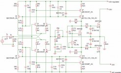
1. I attached the regulator circuit i`m gonna use. hope that`s ok?
2. All your answers ILIMZN have been more theoreticly, is ther any concrete (konkretan) thing I should do? I have transformer that can produce +/-45V and +/-36V so i`ll use +/-369V rails for power stage and regulate +/-45V to +/-40V for the driver stage (I don`t have money for new transformers) so this would be compromise. Hope that` ok...
3.CAscode transistors (Q9,Q10) should have their own heatsinks so:
-would it be better to place them on separate heatsinks or not?
_cascode and css transistors have the same zener diode for a voltage reference, so should I thermaly couple zener diodes with css bjts(BC550/560) or
-I shoul thermaly couple zener diode and css bjt on the cascode`s bjt(BD139) heatsink ?
Thank you all for hel specialy ILIMZN an lineup !
cheers.
I`m wormin up my soldering tools!
Attachments
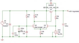
I have used almost same circuit as in your discrete regulator.
Will work well.
You might need to add a compensation cap, to secure stability.
I should suggest you try 470pF or 1nF between Base and Collector of Q2.
Can be ceramic or small film capacitor.
The diode D1, should be other way.
Backwards, against current direction.
Maybe you should change to a lower value of R3 (3k3).
As for now Q2 is biased to only ~0.2 mA.
SInce you alredy have the transformers, the dice have been thrown
Be sure to include quite large filter caps for the auxiliary 45V supply as this is quite close to the 40V desired output. As the transformer is loaded, together with the output stage power supply, the auxiliary supply will droop as well. Adjust the regulator for a clean output under maximum amp load and minimum mains voltage, you may end up with less than 40V, but this is no big deal.
For a regulator, how about this simple tracking regulator I cobbled up, the schematic is from memory so there may be errors, beware! You may need to decrease the 1k resistors from C to B of the BD139/140 if the aux voltage droop is large, or they will run out of base current.
Attachments
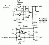
Also, C4, 5, 11, 12 may not be needed (then the 4x4k7 zeber bias resistors can be consolidated into one or two resistors) as the caps in parallel to the zeners already provide a filter and 'bootstrap' current source. This is especially true since you intend on using regulated front end power rails.
ilimzn said:
Ilimzin,
thanks to your exhaustive answer!
Actually I realize that my previous question was a bit pointless when it's so easy to just increase the capacitor level on the driverstage side.
Yes all is very well clear to me in your post, I agree with you on every point!
While reading through your post it reminds me again why I for a long time wanted to use a SMPS with PFC.
Cheers Michael
Ultima Thule said:
While reading through your post it reminds me again why I for a long time wanted to use a SMPS with PFC.
Now, that's a project that is perhaps more complex than the amp it will be powering
3.CAscode transistors (Q9,Q10) should have their own heatsinks so:
-would it be better to place them on separate heatsinks or not?
_cascode and css transistors have the same zener diode for a voltage reference, so should I thermaly couple zener diodes with css bjts(BC550/560) or
-I shoul thermaly couple zener diode and css bjt on the cascode`s bjt(BD139) heatsink ?
bogdan_borko said:3.CAscode transistors (Q9,Q10) should have their own heatsinks so:
-would it be better to place them on separate heatsinks or not?
_cascode and css transistors have the same zener diode for a voltage reference, so should I thermaly couple zener diodes with css bjts(BC550/560) or
-I shoul thermaly couple zener diode and css bjt on the cascode`s bjt(BD139) heatsink ?
Cascode transistor collector current is determined by the BC parts to within 1/hfe, so only the thermal dependence of their hfe will be acting here - the error would be a low single digit % worst case (and probably below 1% real life) so no problem there. hey do not need to be thermally coupled with anything, which means any adequate heatsink will do at your convenience. Short trace routing will probably put them close to the main heatsink so use that if you can.
Thermal dependence of cascode reference voltage does not alter the current through it in a signifficant manner. Again, it comes down to hfe variation with Vce of the BC parts, this is insignifficant in your case as Vce will only change in milivolts.
The thermal variation of the CCS current is another matter, as the cascode stage current also depends on this. Zener tempco breaks even at around 5-6V, below this it is negative, above it is positive. In your CCS the negative tempco of the zener reduces current and the negative tempco of the Vbe increases current, so to an extent you have cancelation. The negative tempco of the BCxxx BJT Vbe in the cascodes tends to increase the current in that stage, but this is reduced by the emitter degeneration there. It could be reduced some, if the oposing collector of your input LTPs (the one now conencted to the rail) was connected in a folded cascode fashion to the emitter of the BCxxx in the cascode, but this folded cascode conenction has it's own implications. In either case, I don't think this is problematic.
What you do want to do is thermally couple the LTP transistors (preferably all of them), or at least keep them very close to each other. This will insure minimum offset drift.
Either way I don't think you have a problem here that would necesitate special measures except for keeping the zener and CCS transistor relatively close to each other, and the two together, in such a place that the references for the + and - rail get heated up (by the proximity of the heatsink, for example) approximately equally - as the tracking of the LTPs is what cancels out your input bias currents and reduces offset.
- Status
- This old topic is closed. If you want to reopen this topic, contact a moderator using the "Report Post" button.
- Home
- Amplifiers
- Solid State
- Question for all mighty ILIMZN and others...