darkfenriz said:
...It can predict basic things, help you with sophisticated designs as well as help you to learn something from nearly scratch without burning silicon....Only, as every tool should be understood and user has to be aware of its severe limitations....inproper realworld PCB.
that's what i mean.....the simulation stuff can give you false hope...it definately is good as a "from scratch" type of thing....but NEVER rely on it solely for a design...in other words before you order those PCB's make sure you do a little bit of real world testing first.
SSSSSSSSSSSSSAAAAAAAAAAAAUUUUUUUCCCCCCCCE
mafoe said:
I was aiming for THDs of 0.000x all over the range of operation. Is that reallistic? Is that good enough? Is there any "golden" THD value one should stay below to name an amplifier "High-End"?
Seeing darkfenriz hasn't answered, maybe I can put an answer in the meantime:
There's no "golden rule"; hi-end audio can have very high distortion figures and still be highly coveted (just check the figures for tubes and you will see). This just points to the fact that there's very little correlation between distortion and acceptability of sound. As others have often said, it isn't hard to design an amp with vanishingly low distortion, however the resulting sound is usually not what you expect! (Plug in an op-amp to jack up the O/L gain and have a look at the simulation - distortion drops to almost zip!)
Cheers!
mafoe said:
...
I guess I'll rework my concept now and keep it a little more simple.
I was aiming for THDs of 0.000x all over the range of operation. Is that reallistic? Is that good enough? Is there any "golden" THD value one should stay below to name an amplifier "High-End"?
Hi
I think you may want either to change your configuration to single ended differential+vas stage ( a la Self's Blameless), or keep is symmetric but lower the voltage dc gain of them.
Also vas cascode needs some care, VAS 'common emitter' transistor has very low Vce the way you did it, the common base transistor must allow some votage drop. on common emitter part.
I've quickly drawn what I mean and what I would basiccaly suggest as a base for your amp's further development. Hope it helps.
About THD... hmmm it's a hard question. Basically below 0.01% should be a goal for 'low distortion amp" up to 20kHz at reasonable levels. However I wouldn't worry much if it jumps to 0.05% or 0.1% at close to clipping (-1dB) because most useful power range is up to 10% for normal music.
Below <0.001 ? Not so hard to do at 1kHz, but at 20kHz feedback is often much lower and thd rises quicly.
Your 2nd order compensation network seems to possibly diminish this effect and enable really low distortion at high freqs. but I am a bit suspicious about 2nd order, probably because my ignorance of this topic. Ask mikeks about it, he's an expert on this.
regards
Attachments
Hi all,
after weeks of playing around with LTSpice, I'm back here with an evolution of my ThermalTrak amp. I gave up the symmetric approach of Slone. My amp is now based on the "blameless" architecture of Self.
Some data:
IS CCS: 3.4mA
VAS CCS: 6.5mA
Vbias: 2.38 volts
Output device Iq: 38.2mA
The LTSpice THD simulations (0.01W, 1W, 100W output at 8 Ohms) show promising values in the 0.000x range between 80Hz and 5kHz, rising up to only 0.009% at 40kHz. The slew rate is approx. 38V/µs rising and 45V/µs falling.
LTSpice tells me about increasing distortion at low freqs (< 100Hz). Do you know why? I can compensate the effect by using strangely large capacitors at the input and in the NFB path. I guess in real life, nobody would use two 1000uF back-to-back as input capacitor.
After trying and simulating a lot of circuits and component value variations for a V-I-limiting, I wonder if such output protection really works. Yet I havn't found any circuit that cuts the current symmetrically on both halfs of the OPS, with a current limit that is constant with output shorts as well as with 1-Ohm loads, and without tendency to oscillation. Have you really simulated and tested your amp for the output current limiting is working as expected, I mean on both halfs of the OPS? Could you show me some examples (circuits and simulation diagrams)?
In any case, I appreciate your comments and critics.
Thanks and regards,
mafoe
Attachments
You could probably lower distortion into low impedance loads by making it a triple darlington.
I have never worked with that kind of CCS which relies heavily on local voltage feedback. I prefer current feedback, i.e. a fixed Zener voltage on the input and generous emitter degeneration in the transistor, maybe a cascode to increase output impedance. But this may be a personal preference.
Also, there are much better (read more linear) small signal transistors to use, namely by Toshiba and Zetex. There are a couple of "favorite transistor" threads in this forum.
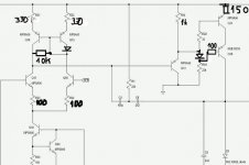
I think it looks good.
It might work very well.
There is only one thing I havent seen before, and I dont understand.
- the purpose of R23, 180 Ohm.
I would prefer using ONLY C15 (220uF) in series with R17 (10kOhm)
between GND and Q10 collector.
It will work, even if you use ONLY R17 (10kOhm) between GND and Q10 collector.
Will flow like 0.15 mA in resistor. ( 1.5V /10k )
And this is nothing.
Very nice, mafoe
consider separate resistors to the ground from current sources, it feels to me that this will be better.
You may also re-consider r-loaded current mirror (Derek Scotland style) I suggested in post 24.
If you put enough attention to correct PCB design, this can turn out very competent design.
By the way, are sanken PCB/spice models available?
regards
Hello again!
After some finetuning of component values and more hours of simulations, I am close to something that could be worth building a prototype. Please have a look on my updated schematics and the technical dossier that I started to write down.
I still wonder about the capacitor disortion which can be observed by simulation at low freqs (<100Hz). Only very large capacitors at the input and the NFB network help to reduce this effect and keep the THD low.
Coming back to some of your suggestions and questions:
Hi darkfenriz:
You are right, seperate CCS grounding resistors look better.
I simulated such loaded current mirror with that diode, as you suggested. Honestly, I don't understand what it is good for and I could not get better simulation results with it. That's why I stay with the simple mirror for the while.
I didn't get your question about Sanken Spice models, what do you mean? I use models from ONsemi's website in my LtSpice simulation.
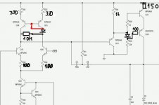
Hi lineup:
The "magic" 10k pull-up R17 helps to speed up the slew rate on the rising edge. I don't know why. I found it just like that. The 180Ohms and the capacitor (R23, C15 now only 100µF) form just another rail filter. At least that's my intention. Could be that's not necessary.
Hi capslock:
You are right. Me too, I would like to parallel 3 output devices but I don't have enough transistors. I got some samples for free but I don't know where to buy ThermalTraks officially here in Germany.
As you suggested I went through several forum threads discussing the choice of transistors. I took the MPSA06/56 because they were used by D.Self in his book and by ONsemi in their ThermalTrak application note. So I hope the MPSA06/56 shouldn't be too bad. Are they?
Regards
mafoe
After some finetuning of component values and more hours of simulations, I am close to something that could be worth building a prototype. Please have a look on my updated schematics and the technical dossier that I started to write down.
I still wonder about the capacitor disortion which can be observed by simulation at low freqs (<100Hz). Only very large capacitors at the input and the NFB network help to reduce this effect and keep the THD low.
Coming back to some of your suggestions and questions:
Hi darkfenriz:
You are right, seperate CCS grounding resistors look better.
I simulated such loaded current mirror with that diode, as you suggested. Honestly, I don't understand what it is good for and I could not get better simulation results with it. That's why I stay with the simple mirror for the while.
I didn't get your question about Sanken Spice models, what do you mean? I use models from ONsemi's website in my LtSpice simulation.
Hi lineup:
The "magic" 10k pull-up R17 helps to speed up the slew rate on the rising edge. I don't know why. I found it just like that. The 180Ohms and the capacitor (R23, C15 now only 100µF) form just another rail filter. At least that's my intention. Could be that's not necessary.
Hi capslock:
You are right. Me too, I would like to parallel 3 output devices but I don't have enough transistors. I got some samples for free but I don't know where to buy ThermalTraks officially here in Germany.
As you suggested I went through several forum threads discussing the choice of transistors. I took the MPSA06/56 because they were used by D.Self in his book and by ONsemi in their ThermalTrak application note. So I hope the MPSA06/56 shouldn't be too bad. Are they?
Regards
mafoe
Attachments
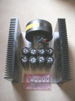
... and here some general concept ideas and a picture.
regards
mafoe
Concept
* monoblock with two bridged 100W (8W) class B amplifiers
* emitter follower output stage using ThermalTrak power transistors, two paralleled pairs per amplifier
* modified "blameless" (D. Self) architecture
* power supply: 2x35V, 500VA toroid transformer, 35A rectifier, 4x27000µF reservoir per rail, 48V nominal rail voltage
* 3mm alu groundplate, 200mm wide, 300mm deep
* two 300mm x 150mm x 40mm heatsinks (left and right)
* front, cover, rear plate: tbd
* PCB horizontally mounted between heatsinks, size approx. 200mm x 220mm, 4 layer FR4 (?)
* vertically mounted transformer, reservoir caps mounted on PCB bottom side (hanging)
* huge input coupling capacitor (1000µF bipolar, paralleled by MKP capacitor)
* huge NFB grounding capacitor (3x1000µF bipolar, paralleled by MKP capacitor)
Attachments
cooling devices
Hello,
see Fischerelektronik in Germany too, one of the "first addresses" for cooling equipment.
Regards, Timo
P.S.
Have a look into the Visaton-Forum, Susie Q, alias Spotnick, alias gegentakt, simulates an interesting amp concept, possibly good for delivering some ideas.
Hello,
see Fischerelektronik in Germany too, one of the "first addresses" for cooling equipment.
Regards, Timo
P.S.
Have a look into the Visaton-Forum, Susie Q, alias Spotnick, alias gegentakt, simulates an interesting amp concept, possibly good for delivering some ideas.
Hi all,
I'm back with an update. After months of playing with LtSpice, I think (or hope) I made it.
The simulation of my amp shows low THD now all over the freqs and signal levels, with decent slew rates, stability, symmetric clipping without strange drops or glitches or rail sticking, fine PSRR, and low noise. All devices seem to stay within their SOAR limits.
Quiescent voltages and currents (input = 0V):
input stage Iccs = 6 mA
VAS Iq = 34.6 mA (through ThermalTrak bias diodes)
V bias = 2.53 V
output Iq = 68.8 mA (through each output device collector)
output DC offset = 870 µV
The next 2...3 months I'll think about overload protection circuits. I am not satisfied with the standard suggestions (V-I limitting).
Any of your hints would be appreciated,
kind regards,
mafoe
Attachments
- Status
- This old topic is closed. If you want to reopen this topic, contact a moderator using the "Report Post" button.
- Home
- Amplifiers
- Solid State
- my project: class B with ThermalTrak