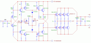
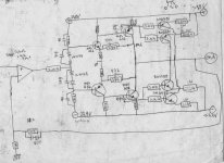
Hy all
I need some comments and advices about the attached
circuit.
It has no feedback but degeneration.
It is a 150W/8Ohm amp il biased with 200mA per output device.
I am not very happy with the 2° stage since it distorts a quite
and has the lone purpose of give the VAS the rigth static voltage.
Any hint? criticisms?
any suggestions about used devices?
thanks in advance
Federico
Attachments
I f you would call transistors with unique names,
will be easier to talk about it,
same with resistors and whatever.
I think you would need a couple of compensation caps.
Maybe across 4k resistor to positive rail, and same in negative.
I am not sure is best to set the gain from within bias circuit.
You can try to test your circuit without 8 power transistors.
Replace them with 2 resistors to create a dummy output.
This will tell if problem is in VAS or comes from output stage.
Hello Federico,
My suggestion:
1. Use JFET, MOSFET. Distortion will be almost 2 harmonic and
canceled in simmetrical topology.
2. Current source instead R-35k for independece DC op. point
from VCC.
3. Use buffer before every VAS for lower distortion.
4. You have 2 VAS stages. Make all of them with gain for lower
distortion in second.
5. Power stage need deep class A in no feedback amp.
6. Use DC feedback for lower and constant DC offset.
PSpice model with 0.05% distortion(Vout=20v, 20kHz, 8 ohm):
Attachments
myhrrhleine said:It looks like there is feedback around the two voltage gain stages, it just doesn't include the follower-outputs.
There is no feedack exept local degeneration.
R25, C3- DC feedback.
rozak said:
There is no feedack exept local degeneration.
R25, C3- DC feedback.
Ummm...
Are we looking at the same circuit?
The one Fredrico posted?
I see a feedback path from the second voltage stage,
through a couple of pots and resistors to the base of the first voltage amp.
That's a feedback loop around the two voltage gain stages.
feedback and the circuit Fredrico posted:
I see a ground connection, so no feedback
Comments - I was going to add a little but I will have to think a bit more and maybe try a sim.
When you say it distorts is this from a real or 'sim' amp? That is have you built it?
Bill
edit: extra comment - Rozak I'm not sure that 'deep' class A is needed.
B Cullingford said:Rozak I'm not sure that 'deep' class A is needed.
'deep class A' would make it easier to get good result
but should be possible to use class AB output stage, too
with a little thinking
lineup said:
'deep class A' would make it easier to get good result
but should be possible to use class AB output stage, too
with a little thinking
From my experience class A is always batter in no global
feedback amp.
If you find the way to use AB with the same result
sand a circuit.
Hi,
thank you all for the comments.
First of all: it is a simulation!
Only when things will go at best in the virtual world I'll begin to tranfer
it to the real world.
yes lineup, I am sorry. I add a new pic with the relevant information.
Since there is no feedback I have not to
compensate the open loop response for stability.
Only, I put a couple of caps to
attenuate a peak in the 1MHz region and after many trial I find
the predriver base to be the best locacation.
The output triple has been tested separately and it perform quite well
(not to forget that it is an AB stage). The problem is the second stage
it does not amplify but, for reason of static voltage levels, it can not
be a buffer so it distorts. How much? a little, from an absolute perspective,
but certainly more of the first stage (a buffer with very low dist) ad the third,
the VAS.
I will be happy to avoid it but I do not see how to do.
Hi rozac, thank you
1. I never design using FET, I don't know them and yes,
it is a limit of mine but soon I'll try.
2. I am trying to keep the number of acrive devices as little
as possible. Distortion is not affected since it is very slow in that point.
what do you mean with "for independece DC op. point
from VCC"?.
3. the VAS distortion is good.
4. I tried to give the second stage some gain and to lower that of the VAS,
but the results were always worst.
5. Sure, class A is better but true class A gives a number
of problems one for all: heat dissipation. I made a compromise:
about 10-12W/4 Ohm in class A (25W/8 Ohm). This give me an acceptable
performance, expecially in the amount of high order distortion components
(obviously not good as pure class A)
6.Thanks, I have implemented your suggestion and it works fine.
What about the time constant? I read somewhere that interference
with audio signal may occur (J.Curl ?)
myhrrhleine
I redraw the circuit to avoid such confusion. Now it is more clear
that there no NFB loop.
a sim, a sim, B Cullingford !!
I analyzed every stage,alone and in the circuit, with res load and with
actual load, and found some facts:
- the major contributors to amp distortion is the output stage when out of class A.
- the second stage follows with a smaller values but I think it cabe done better.
- the other stages have a very very small dist.
rozak, I think class A is always better period.
There is a cost problem however. (maybe not in MOSFET designs, I do not know)
I post this scheme in other forum and I receive some comments.
I'll be happy to hear from you about that.
1) criticisms about the interconnection between gain and bias pots.
2) about the choice of first 3 stages since BC547/557 are 45V devices.
3) about the SOA of MJL4281A/4302A.
I really don't understand the first point since the bias is really not
influenced by the gain pot (just a bit). I think that in a nofeed amp
we need a gain pot to equate the gain of the two channel. Moreover, I have in mind to
add a pot as dinamic balance (2° order harm minimization) as in the attached figure.
I have to say they are right on the second question. devices Q1 and Q2
(and their complementary counterparts) live
at a voltage difference VCE of about 50 Volts, not very variable.
I think to the couple BC546/556 (80Vceo) as a substitute. Any advice?
Q3 instead see a VCE that, at full power, goes from a few Volts up to
100 Volts. Which device is advisable as Q3 in your opinion?
Concerning the SOA I alwais test the amp at full power on a 4 Ohm load (300W)
and trace the V-I curve to verify it is well under the SOA DC limit.
Yes, this is a pure resistive load and I will be happy if some of you
will tell me the values of a reactive load to better simulate the real word
e.g. 4 Ohm paralleled with X uF at 10kHz and 4 Ohm with Y mH serie at 30Hz.
thanks to all
Federico
P.S. for rozak
I went in Israel on my honey moon in 99'. In a nice little village on the sea called
Shavezion. where is Rehovot?
thank you all for the comments.
First of all: it is a simulation!
Only when things will go at best in the virtual world I'll begin to tranfer
it to the real world.
If you would call transistors with unique names,
will be easier to talk about it,
same with resistors and whatever.
yes lineup, I am sorry. I add a new pic with the relevant information.
I think you would need a couple of compensation caps.
Since there is no feedback I have not to
compensate the open loop response for stability.
Only, I put a couple of caps to
attenuate a peak in the 1MHz region and after many trial I find
the predriver base to be the best locacation.
The output triple has been tested separately and it perform quite well
(not to forget that it is an AB stage). The problem is the second stage
it does not amplify but, for reason of static voltage levels, it can not
be a buffer so it distorts. How much? a little, from an absolute perspective,
but certainly more of the first stage (a buffer with very low dist) ad the third,
the VAS.
I will be happy to avoid it but I do not see how to do.
My suggestion:
1. Use JFET, MOSFET. Distortion will be almost 2 harmonic and
canceled in simmetrical topology.
2. Current source instead R-35k for independece DC op. point
from VCC.
3. Use buffer before every VAS for lower distortion.
4. You have 2 VAS stages. Make all of them with gain for lower
distortion in second.
5. Power stage need deep class A in no feedback amp.
6. Use DC feedback for lower and constant DC offset.
Hi rozac, thank you
1. I never design using FET, I don't know them and yes,
it is a limit of mine but soon I'll try.
2. I am trying to keep the number of acrive devices as little
as possible. Distortion is not affected since it is very slow in that point.
what do you mean with "for independece DC op. point
from VCC"?.
3. the VAS distortion is good.
4. I tried to give the second stage some gain and to lower that of the VAS,
but the results were always worst.
5. Sure, class A is better but true class A gives a number
of problems one for all: heat dissipation. I made a compromise:
about 10-12W/4 Ohm in class A (25W/8 Ohm). This give me an acceptable
performance, expecially in the amount of high order distortion components
(obviously not good as pure class A)
6.Thanks, I have implemented your suggestion and it works fine.
What about the time constant? I read somewhere that interference
with audio signal may occur (J.Curl ?)
I see a feedback path from the second voltage stage,
through a couple of pots and resistors to the base of the first voltage amp.
That's a feedback loop around the two voltage gain stages.
myhrrhleine
I redraw the circuit to avoid such confusion. Now it is more clear
that there no NFB loop.
When you say it distorts is this from a real or 'sim' amp?
a sim, a sim, B Cullingford !!
I analyzed every stage,alone and in the circuit, with res load and with
actual load, and found some facts:
- the major contributors to amp distortion is the output stage when out of class A.
- the second stage follows with a smaller values but I think it cabe done better.
- the other stages have a very very small dist.
From my experience class A is always batter in no global
feedback amp.
rozak, I think class A is always better period.
There is a cost problem however. (maybe not in MOSFET designs, I do not know)
I post this scheme in other forum and I receive some comments.
I'll be happy to hear from you about that.
1) criticisms about the interconnection between gain and bias pots.
2) about the choice of first 3 stages since BC547/557 are 45V devices.
3) about the SOA of MJL4281A/4302A.
I really don't understand the first point since the bias is really not
influenced by the gain pot (just a bit). I think that in a nofeed amp
we need a gain pot to equate the gain of the two channel. Moreover, I have in mind to
add a pot as dinamic balance (2° order harm minimization) as in the attached figure.
I have to say they are right on the second question. devices Q1 and Q2
(and their complementary counterparts) live
at a voltage difference VCE of about 50 Volts, not very variable.
I think to the couple BC546/556 (80Vceo) as a substitute. Any advice?
Q3 instead see a VCE that, at full power, goes from a few Volts up to
100 Volts. Which device is advisable as Q3 in your opinion?
Concerning the SOA I alwais test the amp at full power on a 4 Ohm load (300W)
and trace the V-I curve to verify it is well under the SOA DC limit.
Yes, this is a pure resistive load and I will be happy if some of you
will tell me the values of a reactive load to better simulate the real word
e.g. 4 Ohm paralleled with X uF at 10kHz and 4 Ohm with Y mH serie at 30Hz.
thanks to all
Federico
P.S. for rozak
I went in Israel on my honey moon in 99'. In a nice little village on the sea called
Shavezion. where is Rehovot?
Hi Federico.
If your PS is regulated avoid of use CCS.
If not, all currents will be changed with PS volage change.
Buffer betweein first and second VAS can lower distortion
of first VAS too.
Time constant may be 1-3sec. It lower gain of amp from 10Hz
and below.
Interference with audio signal?
Every part interference with audio signal in no-feedback amp.
But if you do it right without any compromise you will
discover how good it can sound.
Rehovot is 20 km south from Tel-Aviv. Very nice place.
Buffer betweein first and second VAS can lower distortion
well, I'll try, thank you
and, pardon, I forgot the pic
bye
Federico
Attachments
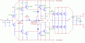
myhrrhleine
I redraw the circuit to avoid such confusion. Now it is more clear
that there no NFB loop.
Thank you.
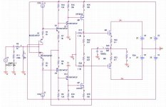
a variation on your circuit
I did some back of the napkin calculations (and then a sim - I like to keep my brain working without the computer) - your second stage is only running at about 0.7mA not enough cuurennt to drive the 4k emitter resistor without distortion, and the 4k collecter will be varying by an equal but oppisite to the input signal, also giving distortion in my experience.
One more calculation - the gain Q3 gives about x20 current gain, so input voltage divided by 4500 (current in Q2) times 20, times 10K is about 100 or 40dB. Do you really need this much? A typical amp (is there is such a beast) has a gain of about x20 or 26dB.
When I first looked at your circuit I thought diamond buffer, CE VAS stage then Output triple. But then I looked closer, almost but not quite.
So my suggestions:
1/ increase the current in Q2 by:
a/ reduce Q1 emitter R to 1K
b/ Q3 emitter R to 330 (including your offset pot)
c/ add a 1000 ohm resistor between the pot and ground
This give us about 4.5 mA current and about 1100 load
2/ Reduce current gain in Q3 by
a/ decrease Q2 collector load to 330
b/ decrease emitter load to 100
I left in the bias and balance pots and'set the gain pot to 8k
My sim gave for 1V in 20V (peak or 40V pp) gave me about 0.05% THD mostly 3rd, not too shabby.
Maybe I should try to build this.
Two other comments:
Your bias pot arrangement - if the pot wiper opens (and this definately happens espicially when setting) the output Iq will go to the max value - hopefully it will not blow up, some amps do


And your current source for Q, the 35K resistor is a wonderful path for PS noise into the circuit, some designers slap a resistor, zener and cap inline, and create its own power supply. I would be tempted to do something a little fancier a nfb local power supply of some sort
Hope this gives you some ideas, happy soldering.
Bill
PS of course the changes apply to the lower transistors as well, and I did not try to optimise the values too much, your transistor models are probably different and neither probably match the real thing exactly.
I did some back of the napkin calculations (and then a sim - I like to keep my brain working without the computer) - your second stage is only running at about 0.7mA not enough cuurennt to drive the 4k emitter resistor without distortion, and the 4k collecter will be varying by an equal but oppisite to the input signal, also giving distortion in my experience.
One more calculation - the gain Q3 gives about x20 current gain, so input voltage divided by 4500 (current in Q2) times 20, times 10K is about 100 or 40dB. Do you really need this much? A typical amp (is there is such a beast) has a gain of about x20 or 26dB.
When I first looked at your circuit I thought diamond buffer, CE VAS stage then Output triple. But then I looked closer, almost but not quite.
So my suggestions:
1/ increase the current in Q2 by:
a/ reduce Q1 emitter R to 1K
b/ Q3 emitter R to 330 (including your offset pot)
c/ add a 1000 ohm resistor between the pot and ground
This give us about 4.5 mA current and about 1100 load
2/ Reduce current gain in Q3 by
a/ decrease Q2 collector load to 330
b/ decrease emitter load to 100
I left in the bias and balance pots and'set the gain pot to 8k
My sim gave for 1V in 20V (peak or 40V pp) gave me about 0.05% THD mostly 3rd, not too shabby.
Maybe I should try to build this.
Two other comments:
Your bias pot arrangement - if the pot wiper opens (and this definately happens espicially when setting) the output Iq will go to the max value - hopefully it will not blow up, some amps do
And your current source for Q, the 35K resistor is a wonderful path for PS noise into the circuit, some designers slap a resistor, zener and cap inline, and create its own power supply. I would be tempted to do something a little fancier a nfb local power supply of some sort
Hope this gives you some ideas, happy soldering.
Bill
PS of course the changes apply to the lower transistors as well, and I did not try to optimise the values too much, your transistor models are probably different and neither probably match the real thing exactly.
Well as they say a piture is worth a thousand words, so here goes - sorry no values on the circuit, my spice program will display them but also shows node numbers and it looks a mess.
The other thing I did is swap the input transistors, the advantage is that if you match NPN1 and NPN2 (and the PNPs 1 & 2) you get no offset (well maybe a little) - otherwise you have to match a npn & a pnp which is hard (impossible?) and then you have to turn that offset pot, which then destroys the dynamic balance and even harmonic cancelation, unless maybe you would like more 2nd.
Bill
Attachments
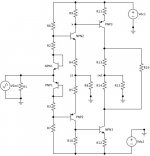
Hi, Michael,
You're right, they are diodes
This one sounds good
You're right, they are diodes
have you tested this kind of inputstage in any real circuit?
This one sounds good
Attachments
I have had the same idea with those 4 input tranies, have you tested this kind of inputstage in any real circuit?
Well along time ago, memory is a little fuzzy, I need to find my notes or look at the input/VAS stage I built but never quite finished (no PCB, dead bug style but no ICs) but I did not do serious listening, at the time I was just experimenting with trying to find very linear nofeedback stages just to see how possible it was. Using transistors as diode is, I believe, a common arrangement for the input of CFP op amps since it solves the offset problem, it is possible to use some open loop and they can sound good, though again my personal listening was limited and along time ago.
As soon as I get my electronics bench set up so I can find things...
Oh and I've got to stop designing and just make something!
Bill
This one sounds good
That's a feedback amp! Quite possible that it sounds good, but we're discussing no feedback, well I guess it didn't take me that long to download on my painfully slow connection and view and say wait a second those are collectors connected to the output, its either a current output or it uses feedback, but it does contain something similar to the input circuit I used. Do not think any that the performance of this circuit helps to understand the other.
Also mine used transistors connected as diodes, this helps match offsets and temp tracking.
More to the point of this discussion... When I was playing around diamond buffers I found that putting small value resistors into the emitter of the input transistor (not connected as a diode) made the linearity worse, I do not think I ever tried bigger Rs such as in the circuit I posted, I quickly tried a sim with smaller R's (100 and 33 I think) and it did not work as well - I've got to think about this, and try it.
Bill
- Status
- This old topic is closed. If you want to reopen this topic, contact a moderator using the "Report Post" button.
- Home
- Amplifiers
- Solid State
- another nofeedback amp