Hi!
I'm looking for a schematic of a all solid state preamplifier, with approx the following requirements:
- only B.J.T. (no I.C.)
- approx amplification factor 20 times
- max output around 30 volt at minimum THD possible
- Output and interstage Capacitor Less
- low output impedance (around 10 Ohm or less)
- 100% No feedback
No problems with the power supply and budget.
Any schematic or at least ideas?
Thank you, regards!
A couple questions.
Why do you need a 30 volt output? Most every power amp out there has an input sensitivity of around 1-2 volts. Or are you planning to drive some sort of unity gain power buffer?
Also, how literally do you mean "100% no feedback"? Do you mean not even an emitter follower or do you just mean no loop feedback?
se
andythefirst said:1)Yes, I need this preamplifier as a voltage amplifier for a current BJT buffer with gain = 0.95 approx.
Ah, ok. Now that makes sense.
")
2)I meant no global feedback, no interstage feedback, but just (if necessary...) local, device feedback.
Ok, I see where you're coming from now.
Any help?
Not sure yet. One more question. Do you have a schematic available for the BJT buffer you're using?
se
Hi!
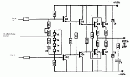
The buffer I should drive, could be, approximately, the one I link to this message. It Is a stage found on the Net, I know lack in output protection and, eventually, a servo.
Carefully implemented, It works very well.
Now, we have to options:
- entering at same time on points "input A", in the preamplifier stage has two outputs,
- or entering, for example, on "input B", if the pre stage has only one output (Complementary BJT)
BUT, I don't want to use coupling capacitors.
And not I.C. Only BJT.
Sorry for beeing not so precise, and again thank you for reply!
Hello and thank you!
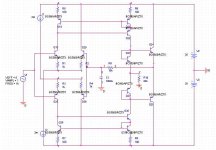
How much is in db the amount of interstage feedback?
In your proposal I must use, according to my schematic, the "INPUT B", is that right?
Is it possible to implemet the two "INPUT A", linking this to collectors of Q23 and Q27 on your schematic?
Thank you in advance for your kind answers!
Pardon, on more question:
I have got Micro Cap evaluation. Will your schematic work on it? And in this case, could you give me the usable file so I can try to simulate and link to it my buffer?
-------------------------------------------------------------------------
How much is in db the amount of interstage feedback?
-------------------------------------------------------------------------
You have only lockal feedback. Gain=R10/R1.
R9, C1 for min. DC ofset.
-----------------------------------------------------------------------
In your proposal I must use, according to my schematic, the "INPUT B", is that right?
-----------------------------------------------------------------------
Right.
-------------------------------------------------------------------------
Is it possible to implemet the two "INPUT A", linking this to collectors of Q23 and Q27 on your schematic?
------------------------------------------------------------------------
No, if you need low Zout
--------------------------------------------------------------------------
I have got Micro Cap evaluation. Will your schematic work on it?
-------------------------------------------------------------------------
No.
For input A:
Attachments
Thank you very much!
According to your knowlege, is there another possibility (maybe easier) to implement the stage?
What do I1 and I2 mean on the schematic?
When you write on transistors "BC550BP/ZTX", what do you mean? Could you be more precise?
Is possible not to use C1 and R9?
Thank you in advance, regards!
According to your knowlege, is there another possibility (maybe easier) to implement the stage?
What do I1 and I2 mean on the schematic?
When you write on transistors "BC550BP/ZTX", what do you mean? Could you be more precise?
Is possible not to use C1 and R9?
Thank you in advance, regards!
andythefirst said:Here is the schematic...
Thanks.
Ok. Reason I was asking is I was thinking of recommending using a step-up transformer and attenuator to be used at the input of your buffer which would eliminate the need for a preamp if your source(s) were capable of driving a 1.5k load. But with the balanced input of your buffer, that rather complicates things a bit.
se
If you want to keep with Aloia spirit of the GY50 why not use the Aikido with 12ax7.
See tubecad.com for several examples of power amp using aikido as the VAS stage.
on a separater point, something I never quite "got" about the italian Bart "T" follower stage is the motivation behind the rail to rai emitter resistors in the predriver-driver as opposed to the original Locanthi T with common emitter resistor. Can anyone explain?
------------------------------------------------------------
What do I1 and I2 mean on the schematic?
------------------------------------------------------------
Constant Current Sourse.
-------------------------------------------------------------
When you write on transistors "BC550BP/ZTX", what do you mean? Could you be more precise?
-------------------------------------------------------------
This transistor is from my simulation library.
You can use any small signal transistors.
-------------------------------------------------------------
Is possible not to use C1 and R9?
-------------------------------------------------------------
You must for this topology at least.
Don't take my schematics us is-it is just theorytical proposition for
starting real project.
Hi and thank you.
I think BJT, especially when you need to use 2 complementary, as in this case to have an OCL, are better with less problems. And it's easier, I think, to have a very low impedence with only 2 BJT.
But a good J-fet OCL non feedback stage can also be considered!
Any ideas?
Regards, A.
I think BJT, especially when you need to use 2 complementary, as in this case to have an OCL, are better with less problems. And it's easier, I think, to have a very low impedence with only 2 BJT.
But a good J-fet OCL non feedback stage can also be considered!
Any ideas?
Regards, A.
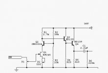
I beg you pardon,
but I ask help to have a little schematic with named components for the purpose I need
I join one schematic I found here but in another thread, but It has two problems:
- The swing is not sufficient. I need 30 volt at very low THD. The problem is also because the power supply cannot be higher with the BJT and Jfet in use;
- Is not Output Capacitor Less. Maybe using two transistor in push pull...?
Any help, ideas?
Attachments
- Status
- This old topic is closed. If you want to reopen this topic, contact a moderator using the "Report Post" button.
- Home
- Amplifiers
- Solid State
- S.s. Preamplifier No Feedback O.c.l.