Hi all
Is there anyone who built the pm-ab1 error correction amp?
I'm not an engineer only diyer.
I'm building one with 2sk1056-2sj60 hitachi pairs, which have different characteristic than the originals, so i changed R7-R11 and R16/R18 to get about 1Vgs on the fets. Now i have 700mA bias current.
My problem is that the bias current decreases when i increase the driving voltage at the input of the opamp. And the output sinus signal becomes
distorted, looks like square wave. The value of the output is only 5Vrms
I have the same results with the both opamps ( AD844, OPA134)
PSU=+28/-28 V
R16/R18= 100R
R8/R9= 33R
R11=130R
R10=100R
R7=2K
So the question is could anyone help me in the procedure how to calculate the values of the resistors, and what should i measure?
thanks.
Attachments
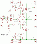
This NP-PMA is difficult to modify. If you want to succeed, you HAVE to built it as "it is" like PMA original design, all components values and types cannot be changed.
Like Ilimzn said, the drop of the VBE multiplier basic is already (Q1+D1+D2+Q2), that is already 2V4 minimum, multiplied by the VBE multiplier effect. You cannot use Lateral mosfets which has below 2V4 total Vgs. Even you remove D1-D4, I think it is not enough for the NP-PMA to work for lateral mosfets (plain without drivers). Q1-Q2-Q3-Q4 needs very tight matching.
CCS formed by Q7+Q9 has to be quite big valued (with R8-11 small valued), because in this NP-PMA, there is no escape route for current, it has to pass Q1 path OR Q3 path, no other escape path like ordinary VBE multiplier.
changed R7-R11 and R16/R18 to get about 1Vgs on the fets.
Dear zsaudio,
based on my understanding and simulations, I concur with ilimzn and lumanauw that the error correction relies on a certain voltage difference between the output transistor and the load. So, should your transistor require less than that, they will not work.
Saying that, I haste to encourage you to acquire the original transistors - they are still available - and build the amplifier. The result is more than well worth it - search under my moniker for my impressions.
After all, I am practicing what I preach as I type this, waiting for some additional parts to arrive. ;-)
Where are you Pavel when people need you!?!
Dear chicco_36,
I cannot speak for Pavel, but as he may not monitor this thread, let me rely my experience.
When I first heard the amplifier, I was so enamored by its performance that I have been badgering Pavel about re-designing for different output transistors. Pavel tried, but none of the transistors simulated to his requirements.
Consequently, I am afraid that the version he designed will remain the only one endorsed by him.
M
Could you show me any dealers, who sell these MOSFETs on the net?
Dear zsaudio,
are you familiar with Google?
http://www.google.com/search?hl=en&q=2SK413
http://www.google.com/search?hl=en&q=2sj118
You can also try Borbely.
M
Thank you the tip Mefistofelez, yes i know google, but i'm afraid for fake devices. I don't know if exists fake ones, or not on the markets, but i wouldn't like to buy fake ones. I'm not at home in Hitachi's and Toshiba's devices. I have read that it's better to be careful. So i'd like to know a trustful dealer.
Every perceptions are welcome in this issue.
Thank you gents.
Every perceptions are welcome in this issue.
Thank you gents.

- Status
- This old topic is closed. If you want to reopen this topic, contact a moderator using the "Report Post" button.
- Home
- Amplifiers
- Solid State
- question about pm-ab1