Hi,
I posted a question on this a few months back, it still remains an unsolved problem for me though.
I built a Quad 405-2 amplifier, with the well known mods done to it ( OPA134, MJ21194's, more capacitance)
Also an HT of 55v (5v above the original design).
It works very well without a load doing 80V pk-pk, 100w into 8 ohms.
But as the frequency goes up (roughly at 10khz and above) or as the load is reduced from 8 to 4 ohms the oscillation gets worse until the waveform becomes almost jagged. With oscillation in the order of several Mhz on positive cycles, crossover distortion becomes visible too.
I actually gave up on it before but have been away at university for a while and now want to get it working.
Somthing is wrong but i cant find out what, i have snubbersied, ferrite beaded, base stoppered but still cannot solve the problem.
Cheers
Craig
ok i just got rid of the oscillation problem by putting 680nf in // with the speaker now it doesnt oscillate at all even under full power into 3 ohms.
I still get jagged waveforms on high frequencies.
I am sure that the capacitor solution is a terrible one but it works well enough and doesnt attenuate the signal within the 20khz range at all so im happy .
.
What might be causing the jagged sine waves?
Cheers
Craig
I still get jagged waveforms on high frequencies.
I am sure that the capacitor solution is a terrible one but it works well enough and doesnt attenuate the signal within the 20khz range at all so im happy
.What might be causing the jagged sine waves?
Cheers
Craig
Hi Craig,
Agree with Chris - could be the layout of the amp is causing instabilities. Could you post what the "jagged" waveform looks like? Doesn't have to be a true picture, even just a hand-drawn figure might help.
Also, try 'scoping the supply waveforms going into the OPA134, see if you can spot some niggles when the oscillation happens...
Cheers!
Clem
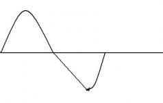
As i remember from last time i tried to repair this, the oscillation i get appears all over the PSU grounds and on the output at about 5mV pk to pk but gets worse at higher frequencies.
I am rebuilding the PSU and rewiring the lot today to eliminate any possibilities from this area.
I will try and do a sweep of the frequency response and get current readings from the supply as soon as its back in one piece.
The only problem i forsee in the sweeping is that i only have one ancient function generator and i think i need 2. Ill try and get some results today or tomorrow.
Also here i a picture of the waveform at higher frequencies with the oscillation also present.
Thanks
Craig
Attachments
Craig,
Did you have the usual 0.1uF + 10 ohms across the output? If not, try that, or even keep the 0.68uF but put a 5 or 10 ohms in series. It probably still gets rid of the oscillation without loading the amp in the audio range too much.
Did you put in an output series inductor?
Jan Didden
Did you have the usual 0.1uF + 10 ohms across the output? If not, try that, or even keep the 0.68uF but put a 5 or 10 ohms in series. It probably still gets rid of the oscillation without loading the amp in the audio range too much.
Did you put in an output series inductor?
Jan Didden
Hi Craig,
I see you have been struggling with this amp for months now. This link is a brilliant bit of work on modding the 405 which may give you some info on how to solve the problem.
http://www.dc-daylight.ltd.uk/Valve...on/405_Qw_6.pdf
I would echo Janneman's thoughts on the zobel network but you might need to make the resistor lower than the 5 to 10 ohms he suggests. The standard 0.1uf and 10 ohms will not do much.
The waveform you have posted is classic slew rate limiting. I note from the above link that the 405 does not have good figures for its slew rate spec.. Perhaps you are expecting too much from the design. It would be worth noting the slope of the straight bit of the distorted sine waveform (in V/uS) and comparing that with the spec.
The presence of numerous inductors and capacitors for compensation shows that the design is touchy and any deviations from non-standard may be troublesome oscillation wise!
Thanks for replies everyone.
I have rewired the PSU and one channel alone with very short thick wire so thats fine now.
Here are current readings taken from the positive rail at various input frequencies;
10v pk-pk output into no load;
100hz = 89.7mA
1kHz = 89.8mA
17.5K = 89.4mA (first obvious signs of triangulation appear)
22.5K = 87.9 mA
60k = 86.3mA
with 5 0hm load, no input measured 86.5mA idle;
100hz = 90mA ( wave already looks bad)
10Khz = 89.9mA
20K = 89.2mA
25K = 88mA
30K = 87.3mA
60K = 86.5mA
As for the op amp supply it looks horrible even though it is transistor regulated, the input signal appears there with lots of oscillation all over it.
Jan yes i have the 0.1uf 10 ohm network in place, and have tried a few values of output inductor// resistor too but i still get the same trouble.
consort_ee_um thanks, i pretty much built my amp using tips from those sites they are very good.
I cant find my PCB layouts, i hadnt backed them up and probably deleted them a while ago (never thought id need them again..doh)
Thanks
Craig
I have rewired the PSU and one channel alone with very short thick wire so thats fine now.
Here are current readings taken from the positive rail at various input frequencies;
10v pk-pk output into no load;
100hz = 89.7mA
1kHz = 89.8mA
17.5K = 89.4mA (first obvious signs of triangulation appear)
22.5K = 87.9 mA
60k = 86.3mA
with 5 0hm load, no input measured 86.5mA idle;
100hz = 90mA ( wave already looks bad)
10Khz = 89.9mA
20K = 89.2mA
25K = 88mA
30K = 87.3mA
60K = 86.5mA
As for the op amp supply it looks horrible even though it is transistor regulated, the input signal appears there with lots of oscillation all over it.
Jan yes i have the 0.1uf 10 ohm network in place, and have tried a few values of output inductor// resistor too but i still get the same trouble.
consort_ee_um thanks, i pretty much built my amp using tips from those sites
they are very good.I cant find my PCB layouts, i hadnt backed them up and probably deleted them a while ago (never thought id need them again..doh)
Thanks
Craig
Hi Craig,
It really looks like a predriver or earlier does not have enough current. It's slewing as noted before, the negative side. I ran into that once in a signal darlington stage. The fix was to increase the current to the first transistor (resistor E-B on the second transistor).
-Chris
It really looks like a predriver or earlier does not have enough current. It's slewing as noted before, the negative side. I ran into that once in a signal darlington stage. The fix was to increase the current to the first transistor (resistor E-B on the second transistor).
-Chris
Ok ill give this current increase thing a try, the hard thing being which part of the circuit is lacking in current.
Looking at the measurments i posted ages ago on this diagram it looks like very little curent is flowing anywhere within the circuit, which is very wrong for a class A amplifier, right?
I have a feeling the problem lies between the 2N5551 and the base of Q15 (BD244C).
The CCS loading the first transistor should be providing 4mA to the 2N5551 under the original quad design.
1.05V at its base - 0.6V, leaves 0.45V dropped accross the emitter resistor of the CCS so 4.5mA is flowing.
is this right? if so the idle current stays roughly the same or even less up until BD244C's base. And the supposedly class A drivers arent even switched on.
Where should i start?
Hope that made sense, i am still learning electronics.
Thanks all
Craig
Attachments
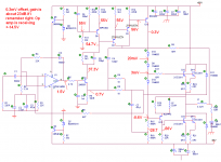
Actually this circuit is insane. I can't imagine how a thing with an op-amp and five transistors (most of them common-emitter with its corresponding pole) inside a feedback loop could have ever been made stable.
Note that five transistors without any op-amp are already hard enough to stabilise.
Also, I don't remember exactly the original circuit, but I think that this one has substantial differences that may make it inherently instable.
Note that five transistors without any op-amp are already hard enough to stabilise.
Also, I don't remember exactly the original circuit, but I think that this one has substantial differences that may make it inherently instable.
I do agree with you that this is a bit of an odd circuit. I cant get any scope readings that make sense to me, the signal goes unrecognisable at Q10's collector then amazingly is restored at the output of the amp.
Also it will be difficult to break the large feedback loop to track down the stage causing the problem anyway.
I think this amp probably deserves packing away now never to be exhumed again, ill save the PSU for another project though.
(wish i had built a KSA50/100, much easier to fault find)
Thanks for all the posts.
Craig
I have to admit that I would enjoy troubleshooting such a circuit I would keep trying if I was you, altough there is nothing you can do until you understand exactly why the waveforms look so strange.
EDIT:
I have just noticed that one of the miller capacitos is missing in your schematic and the other is connected in another way.
This schematic of a modified 405 shows the same difference :
http://www.mver.as.ro/QUAD405reborn.gif
However, look at the original schematic:
http://www.geocities.com/quad_esl63/images/schematic/power405.jpg
I hope this to be a good hint...
I would keep trying if I was you, altough there is nothing you can do until you understand exactly why the waveforms look so strange.EDIT:
I have just noticed that one of the miller capacitos is missing in your schematic and the other is connected in another way.
This schematic of a modified 405 shows the same difference :
http://www.mver.as.ro/QUAD405reborn.gif
However, look at the original schematic:
http://www.geocities.com/quad_esl63/images/schematic/power405.jpg
I hope this to be a good hint...
Now I understand how they were able to make the circuit stable
There are two nested feedback loops. The inner one receives its input signal in the base of Tr2 through R12 and the feedback signal in the emitter of Tr2 trough R20 and R21. Thus, the collector current of Tr2 is proportional to the difference between the output voltage of the op-amp and a fraction of the output voltage of the amplifier itself. This forces a closed-loop voltage gain of 3.78 in this inner loop, so the output of the op-amp must swing at least +-13V in order to get a +-50V voltage swing at the output of the amplifier.
The outer loop is controlled by the op-amp and employs split feedback techniques. The output voltage of the whole amplifier is low-pass filtered through R5 and C2, and then applied to the inverting input through R4. The output voltage of the op-amp is high-pass filtered and also applied to the inverting input through C4 and R6. This means that more feedback is taken from the output of the amplifier and less is taken from the output of the op-amp as frequency decreases.
In order to troubleshoot such a circuit, the first thing that I would do is to bypass the split feedback system and the own op-amp. This is achieved by replacing C2 by a much higher value (lets say 1.000uF 16V) and shorting C4. Then the op-amp will behave as a harmless DC servo and won't affect amplifier stability.
And the second thing that I would do is to increase the closed-loop gain of the inner loop to check for phase margin issues. A 6dB increase is achieved by either disconnecting R20 or R21, and to further increase it the value of the remaining resistor should be increased. Note that the required voltage swing from the output of the op-amp is readuced as the gain of the inner loop is increased.
Also, note that all the component labels and values that I mention are referred to the original 405 schematic, so you will have to find the corresponding components in your modified schematic.
- Status
- This old topic is closed. If you want to reopen this topic, contact a moderator using the "Report Post" button.
- Home
- Amplifiers
- Solid State
- Oscillation under load