Hi all,
For the last four months I've been simulating alot in LTspice, my knowledge about ampdesign has grown alot. But I'm still an amateur, and probably will stay also.
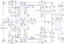
I wanted to desing an amp with MOSFET output devices and JFET input devices. I've used always MOSFET's in my previous diyamps, and I'm very pleased with them. Some people made me curious about using JFET's as input.
Because JFET diff pairs don't have much gain, I had to use a differential VAS also. The total closed loop gain is about 13000.
I used cascoded VAS'es. Because the voltage drop is big with a cascoded VAS and even bigger with a diff cascoded VAS (+R48 and R49), I use a +-80V regulated PS for the front stage.
I want to use the inverting input of the diff pair also for a balanced input signal. When I'm not using this, R33 has to be connected to ground.
Some numbers:
*current throught each leg of diff input: 1.7mA
*current throught each leg of diff VAS: 22.5mA
*current throught EF (MJE15030/31): 37.4mA
*idle current throught MOSFET's: +-140mA
*Slew Rate is +-100
*Closed loop Bandwith= +-110kHz
Please critizise the design, when you see error's of things that can be beter, tell me.
Greetz
Ben
For the last four months I've been simulating alot in LTspice, my knowledge about ampdesign has grown alot. But I'm still an amateur, and probably will stay also.
I wanted to desing an amp with MOSFET output devices and JFET input devices. I've used always MOSFET's in my previous diyamps, and I'm very pleased with them. Some people made me curious about using JFET's as input.
Because JFET diff pairs don't have much gain, I had to use a differential VAS also. The total closed loop gain is about 13000.
I used cascoded VAS'es. Because the voltage drop is big with a cascoded VAS and even bigger with a diff cascoded VAS (+R48 and R49), I use a +-80V regulated PS for the front stage.
I want to use the inverting input of the diff pair also for a balanced input signal. When I'm not using this, R33 has to be connected to ground.
Some numbers:
*current throught each leg of diff input: 1.7mA
*current throught each leg of diff VAS: 22.5mA
*current throught EF (MJE15030/31): 37.4mA
*idle current throught MOSFET's: +-140mA
*Slew Rate is +-100
*Closed loop Bandwith= +-110kHz
Please critizise the design, when you see error's of things that can be beter, tell me.
Greetz
Ben
Attachments
PCB split
Is there any problem when I would split the PCB in three parts, namely;
1) the total front stage, power supply +-80V
2) 4x 2SK1058 with MJE15030
3) 4x 2SJ162 with MJE15031
I can't make it out of on big PCB. But I can assemble these three parts close to eachother with very short wires.
Is there any problem with osscilation or something else maybe.
This could save me alot of money when I would do it wrong I guess.
Cheers
Ben
Hi Ben, rail voltage at VAS must be little bit higher, cca 82-83 V... Serial resistors at gates should have lower walue ( 39 at P and 47 at N ) - amp stay stabil and SR will be much higher... Give some RC compensation from VAS to minus input and give out this one from output... And design of PCB will be very important... ")
Hello!
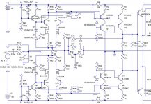
If I'm not mistaken, I think you may be able to delete transistors Q1, Q11, Q9, and Q10.
==> You're taking the differential output of your input stage into another differential input of the VAS stage, but one side of the differential VAS stage is doing nothing (it has its outputs grounded at the collectors of Q1 and Q9).
Unless I'm missing something, I think you could simplify the VAS stage to save on a little cost and board space for the PCB.
Upupa Epops,
Do you mean to lower the gate resistors from the MOSFET's? (Not JFET's). That's the first time I see these low values for gate stoppers in lateral mosfet design's?? Are you sure? In my last project I blew up 10 x2sk1530/2SJ201 due to, to low gate stoppers -> oscillation.
I've experimented alot with this NFB network. Taken the feedback from VAS will lead to a more stabil amp, but THD will rise.
Do you mean by "and give out this one from output", that I have to omit this feedback from the output and take only feedback from the VAS? Have maybe a link to a good amp that is using this kind of NFB?
I'm aware that the voltage for the front stage must be floating round the same ground. But you say that they have to be in series, in my design I'll do this in serie. But is this really necessary?
rtarbell,
Im' sorry to say, but yes you are missing something. Take a good look at the shematic, R48 and R49 can be replaced by two current cources, than you will have the same as in the differential input. R48 and R49 are serving as current source. Without these transistor's, the closed loop gain would be +-3000 instead of +-13700.
Yes, I mean gate stopers at power mosfets - if you give them ASAP to gate, amp will be stabil. And I don't mean all feedback, but only compensation... And floating supplies are neccessary - if you make VAS's voltage regulated, by full load, when voltage at output rails will drop, voltage at VAS will be too high and amp will be not stabil... If you can, I will send you my schematic and you can take there inspiration...send me a mail, all is to large...
Thanks for the mail.
You did me realise that the capacitor (C8, like by Leach http://users.ece.gatech.edu/~mleach/lowtim/fdbk.html)
to ground, better not can be used with mosfet's. With a mosfet design it is possible that the mosfet's are oscillating (or starting to), and with this capacitor the error correction won't be able to "see" this oscillation.
Am I correct?
Ben, mosfets can oscilate easy at hundreds MHz and it you can't "repair " by any global feedback - you must remove basic reasons of this oscilations - constuction must be very careful and you must hold basic aspect for suppression of instability - ASAP short traces at PCB and good grounding...
lineup said:Looks like that, at first sight.
But if you look at power supply - to the left -
you see VAS is a differential stage.
With a common resistor from supply.
That may be true but it still seems odd to terminate one of the differential outputs in the VAS stage. One could just as well have used current mirrors in both differential inputs and a symetric non-differential VAS. Less complex, and not much difference in gain.
Do you mean about R67 ? If you do this , crossover distortion of output stage will not be repaired by feedback . I have ever done like this ,and I must left that idea . Do you try ? and tell me resultAnd what do you think is the best to take the NFB from, wright after the diff VAS, or after the emitter follower. I can split the 33R resistor in 2x16R, and use the midpoint here.
I've made a NFB network as leach does it. The output signal is much nicer with high fequenc's and capacive loads.
The normal NFB network is not much changed, except for the 47K resistor, this one is split in two, with in the midpoint a capacitor to ground. This one is needed to not let the gain decrease to much in high frequency's.
I don't know whether I can omit the 4.7P cap and the 1.5K resistor in the original NFB network?
Upupa Epops,
Do you mean by "By my opinion is it better from VAS and stability of EF " hold " by local feedback...", that I have to put some local feedback from EF to VAS? Like C22 and C23 in your shematic(DPA386)?
Good thinking of you Thanh, the sim's show higher THD with the NFB taken from the midpoint.
Thanks for all the help
Ben
Attachments
Bensen ! I tried to do this with real amp . Crossover distortion make me crazy  .Do you like a non-switching output stage ? I will post it . But it show many TIM in the pspice .
I'm quite happy with Symasym5 ( with cascode input ) . I also intend to convert Symasym5 to a symetrical amp with differrential vas .
.Do you like a non-switching output stage ? I will post it . But it show many TIM in the pspice . I'm quite happy with Symasym5 ( with cascode input ) . I also intend to convert Symasym5 to a symetrical amp with differrential vas .
Hi Benson,
Your Q1,9,10,11 don't do anything. You don't need them.
R11,12 are best removed (anytime) as they just waste gain which could be used for NFB and increase modulation (distortion). They're a hangover from the TIM dreaming.
NFB from the output corrects the worst ERRORS in most amplifiers - the output stage ones. You don't wan't to be listening to these as Thanh says. And they're load dependent so variable.
Cheers,
Greg
- Status
- This old topic is closed. If you want to reopen this topic, contact a moderator using the "Report Post" button.
- Home
- Amplifiers
- Solid State
- Fully complementary FET-in FET-out design