HI all ,,
I found this mosfet amp that i wanna use to power my 80 watt tweeters via a 2 - way linkwitz riley x-over with a crossover point of 3.1 Khz,
I simulated the circuit in using circuit maker 2000 and in worked wonderfully!!. The problem is I build the project on Vero board, and it does not work I get a bad dc offset on the outputs, which fries my mosfets I don’t understand why its doing this ??I checked my wiring 10 times .......
I used a +/- 15 Supply just to test and I thought maybe the supply is to weak and I applied the full +/- 30Vdc and bang the mosfets fried Instantly
Please Help ,
Thanks in advance…
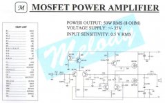
Amplifier diagram attached.
I found this mosfet amp that i wanna use to power my 80 watt tweeters via a 2 - way linkwitz riley x-over with a crossover point of 3.1 Khz,
I simulated the circuit in using circuit maker 2000 and in worked wonderfully!!. The problem is I build the project on Vero board, and it does not work I get a bad dc offset on the outputs, which fries my mosfets I don’t understand why its doing this ??I checked my wiring 10 times .......
I used a +/- 15 Supply just to test and I thought maybe the supply is to weak and I applied the full +/- 30Vdc and bang the mosfets fried Instantly
Please Help ,
Thanks in advance…
Amplifier diagram attached.
Attachments
Hi,
540 is a vertical FET and needs a thermal compensation scheme to keep the bias controlled. Your schemematic has no source resistors which makes the problem even worse. Lateral Fets could work successfully with this layout because they become negative temp coef at about 100mA and above.
Some people use VFETs but the circuit must be designed to suit.
Lateral FETs are much more expensive £4 vs £0.60 in UK.
Its strange the circuit looked very promising when i used circuitmaker 2000,also i thought a mosfet dont need any bias due to the high input resistance?, the minimal drain to source resistance is about 0.1 ohms so why would i need source resistors ?? is this a bad design if true then i can sleep in peace,without having to diagnose an amp that is not worth troubleshooting. i spend all weekend thinking it will work but sunday i gave up !!!
I thought mosfets are tuff transistors and fast too thats why i use the amp for high frequency applications,not to mention its attractive
design cost and power output .Is there an alternative to this design with the same design cost and output it will really help me a lot.
I thought mosfets are tuff transistors and fast too thats why i use the amp for high frequency applications,not to mention its attractive
design cost and power output .Is there an alternative to this design with the same design cost and output it will really help me a lot.
There is also another thread about this amp.....well it drifted a little lately....
http://www.diyaudio.com/forums/showthread.php?s=&threadid=40079&perpage=10&pagenumber=1
Ciao, Tino
http://www.diyaudio.com/forums/showthread.php?s=&threadid=40079&perpage=10&pagenumber=1
Ciao, Tino
Vertical MOSFET's
Almost all devices today are verticals (IRF, HARRIS, ....) with very few being horizontals (Renesas = formerly the Hitachi, Exicon, and some BUZ..)
The horizontals have a temperature coefficient which leads to lower transconductance when getting hotter even at fairly low currents. This way, you can bias them "just wit a pot", they will not run away.
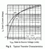
With verticals suitable for power amp outputs, forget this, as already stated. The current where you get negative temperature coefficient is VERY high. Look for data as attached. >10A for zero tempco of an IRFP240...
You need to adapt the circuit, eg using a VBE (VGS) multiplier.
Or use horizontal devices, such as the Renesas 2SK1056/2SJ160, which were used in the original design.
Tino
Almost all devices today are verticals (IRF, HARRIS, ....) with very few being horizontals (Renesas = formerly the Hitachi, Exicon, and some BUZ..)
The horizontals have a temperature coefficient which leads to lower transconductance when getting hotter even at fairly low currents. This way, you can bias them "just wit a pot", they will not run away.
With verticals suitable for power amp outputs, forget this, as already stated. The current where you get negative temperature coefficient is VERY high. Look for data as attached. >10A for zero tempco of an IRFP240...
You need to adapt the circuit, eg using a VBE (VGS) multiplier.
Or use horizontal devices, such as the Renesas 2SK1056/2SJ160, which were used in the original design.
Tino
Attachments
The hell with that mosfet amp it going to give me grey hairs if i pay futher attention to it , why does ppl put diagrams like those on the internet in the 1st place,,
I think i found a good amp ,, P3A looks good !!! any comments on this amp ??This will power my tweeters very well i think ,,
I think i found a good amp ,, P3A looks good !!! any comments on this amp ??This will power my tweeters very well i think ,,
Upupa Epops said:Or BUZ 900 - 906...
Or 2SK1058/2SJ162, I think this is one of the best audio-mosfet pair even manufactured.
Hi Reactance,
As has been said the lateral MOSFETs need a tempco tracking bias chain to reduce Vgs accurately as they warm up.
When I designed my Simple Killer Amp using IRFP240/9240 pairs I characterised the devices thoroughly over 100pcs before designing the amp. The tempco of these at 50mA bias is -5mV/deg C. I then designed a cct to track these at that rate and the result is very stable bias with temperature. Having done that I didn't need source resistors and was able to take full advantage of the rugged good performance of these devices.
Hope that helps.
Cheers,
Greg
Hi, Reactance,
Thanks for swearing a schematic that comes from my website. If you buy the real kit (which the pcb is carefully planned and the components are carefully matched), you will not swearing on my schematic.
The schematic is put on internet is not for you to clone, or it is put there to give you grey hair, but for explaining what is inside the kit. I do not expect people to hijack the schematic and then swear on it.
Thanks for swearing a schematic that comes from my website. If you buy the real kit (which the pcb is carefully planned and the components are carefully matched), you will not swearing on my schematic.
The hell with that mosfet amp it going to give me grey hairs if i pay futher attention to it , why does ppl put diagrams like those on the internet in the 1st place,,
The schematic is put on internet is not for you to clone, or it is put there to give you grey hair, but for explaining what is inside the kit. I do not expect people to hijack the schematic and then swear on it.
Thanks for swearing a schematic that comes from my website.
Try building an amp and find out after 2 and a half hrs of checking and rechecking ur work, it does not work only bad dc that melts ur money quiker than a blink of an eye u feel humiliated and stupid as well as robbed in a sense that u wasted your time money for an audio amplifier circuit that looked promising.At least have the decency to tell people it does not function correctly.
NO WHERE ON YOUR WEBSITE DO U SPECIFY THIS !!!!!!!!The schematic is put on internet is not for you to clone

From now any diagram that comes from u will remain questionable
In terms of readability and performance.
Learned a lot from this none the less.
Never build "easy looking amplifers" with no support from others.
Upupa Epops said
It is original schematic designed with old Hitachi SK/SJ , which some nitwit " redesign " for vertical IRF... Andrew is correct, without thermal compensation it will goes into " heaven "....
Hi, Reactance,
Thanks again for being so nice to me.
In your simulator it works fine, then why is it don't work in your clone? Do you have a slight thinking that you must have missed something, before you write something that shows everyone about how you are being so nice to me?
If you just try different combination of VBE's of BC556 AND D667, you will find a pair combination(s) of both that works fine.
The key is this : this is a "dual differential" design WITH both legs of differential is used. You HAVE to match the performance of the first differential (BC556) AND the second differential (D667). Matching only the BC556 is not enough, because both legs of the differential is used in the first and the second stage.
I admit that this topology is not easy to implement, but once you have done it, it sounds very nice. This topology is not so forgiving like ordinary 3 stages amp (where the VAS is single loaded). This topology requires matching like the AlephX (I mean in the difficulty of the matching transistor). Also the same difficulty as the Hiraga types of CCT (But I don't recall anyone being so nice to Grey Rollins or Hiraga like Reactance do to me)
This topology is sensitive to VBE mismatch, because both legs of the differential is used, both in the first differential, and the second differential (balanced VAS to some).
Imagine this. If the transistor's gain is 50X. 1mV mismatch in the first (or second differential, where the other pair is perfectly match) will result in 50mV mismatch in output stage. This topology is not forgiving like the single loaded VAS, where the DC offset is determined ONLY by the matching of the differential. VAS only follows in that configuration, DC offset is dictates alone by the differential pair, but not with this type of circuit. Can you imagine what happens if the first and second differential transistors are not carefully matched? You will end up in something like 2-3V DC offset.
If you don't like matching the transistor, there is one easy way to make it properly. I don't know what configuration in your clone. The voltage rail is sensitive too.
Remove the 12K resistor (or use smaller value, say 4k7). This way you will not have to match anything.
I really hope I can help you implementing this cct. Or you will behave more and more nice to me?
Hi Upupa Epops,
You are right, this schematic is lack of VBE multiplier. It will work fine with lateral FETs.
The first intention of this amp is to make an amp that is not too expensive. Look at the price of the PCB and full kit. But I slipped in thinking, it turns out difficult in matching the components, so even a nice people like Reactance is behaving so nice to me.
If he just BUY the kit, he will turn into bad man, not the so nice man like this time.
Ok, i admit i was a bit rude to u sorry man.I really hope I can help you implementing this cct. Or you will behave more and more nice to me?
I apologize for saying to hell with your diagram.
Ok then so what should i do to make this amplifier work ??
Any help u gots the diagram what now ??
Also the circuit i used was simulated using ideal components, spice is very tricky, sitting on the work bench is is always different from spice.
but its close enough though i dont have extentive knowlege in this area of circuit simulation.
Cool man no hard feelings ok ,,,,
I still hate the smell of burned output transistors,,,
Hi Luman,
just admit the circuit as published does not work and either say so on the schematic or remove the schematic from your site.
I've think about it. It's gone now.
Hi Lumanauw,
Is the schematic representative of your kit? I'm genuinely interested in how the quiescent current remains stable with just a pot for bias. Does the tail current of the balanced VAS take care of the change by reducing when warm? Or have you just found in practice that it's not a problem and bias just drifts up by a small amount?
Is the schematic representative of your kit? I'm genuinely interested in how the quiescent current remains stable with just a pot for bias. Does the tail current of the balanced VAS take care of the change by reducing when warm? Or have you just found in practice that it's not a problem and bias just drifts up by a small amount?
- Status
- This old topic is closed. If you want to reopen this topic, contact a moderator using the "Report Post" button.
- Home
- Amplifiers
- Solid State
- 50 watt MOSFET AMPLIFIER