Having just browse through Douglas Self book, I'm just excited want to tried out his blamesless amp, which measured very well. I'm using MJE340 instead of BC550C as phase splitter where I would mount it on top of power transistor for better thermal tracking. Can this work?
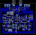
Attached is my layout and pls give comment.
Thank you.
")
Attached is my layout and pls give comment.
Thank you.
Attachments
I didn't think there was any phase splitters in this design. Are you sure you understand the design? Perhaps you mean the Vbe multiplier (bis generator)? In which case yes it would be good to mount it in thermal contact with the output devices. I'm sure this part is very well covered in the book/article as he has tweaked the Vbe multiplier for certain thermal characteristics.
A blameless amplifier can have either an EF or a CFP output
If EF, which is yours, the thermal sensing transistor should be sticked to the top of one of the output transistors. This is one of the biggest difference with almost all amplifiers which were commercialized before the publication of Self's works.
Do not forget the capacitor across the emitter resistance of the drivers.
All this is very clear in Douglas Self's book.
~~~~~~ Forr
§§§
sorry for the confusion. It is indeed a bias generator. Always confuse with the name.
The blameless schematic can be found here (Figure 13).
http://www.dself.dsl.pipex.com/ampins/dipa/dipa.htm
I made a small modification by adding a low pass filter to the supply so that input stage and bias generator stage supply voltage will be more stable.
In the original schematic, the bias generator transistor is MPSA06 (TO92 package), which I find it to be harder to mount for thermal tracking on heatsink, so I change this to MJE340 (TO220) package for easier mounting on top of power transistor. Will this affect the circuit performance?
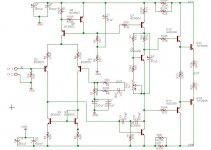
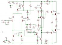
Attached is the schematic. Hope it is clearer now.
Pls also advice me on the PCB routing as I get lots of hum noise from my previous layout.
Thank you.
The blameless schematic can be found here (Figure 13).
http://www.dself.dsl.pipex.com/ampins/dipa/dipa.htm
I made a small modification by adding a low pass filter to the supply so that input stage and bias generator stage supply voltage will be more stable.
In the original schematic, the bias generator transistor is MPSA06 (TO92 package), which I find it to be harder to mount for thermal tracking on heatsink, so I change this to MJE340 (TO220) package for easier mounting on top of power transistor. Will this affect the circuit performance?
Attached is the schematic. Hope it is clearer now.
Pls also advice me on the PCB routing as I get lots of hum noise from my previous layout.
Thank you.
Have you read the rest of the book on good layout practices? I think you need to revisit that bit as I can see you sharing decoupling and input ground traces.
I would also significantly reduce your low-pass filter resistors to maybe 100 ohms (from 680) each as an absolute maximum as they will be strangling the VAS stage.
I would also significantly reduce your low-pass filter resistors to maybe 100 ohms (from 680) each as an absolute maximum as they will be strangling the VAS stage.
Your schematics is a bit different form D. Self's blameless.
There is no CC input at the VAS.
Beware that the two pole compensation can lead to instabilities. Build your amp with only with a simple Miller compensation first (I abandon the two-pole compensantion the first time I tried it because of oscillations. My boards were from Signal Transfer, I do not think the recent ones include the two pole compensantion in the layout).
I glued the small thermal sensing transistor on top of one of the TO3 power transistor. Theorically, the use of the MJE340 should not change much, this is what is done with the CFP output stage, in thermal contact with one of the drivers.
Take acount of the other remarks of the thread about the decoupling, the schematics and the layout .
~~~~~~ Forr
§§§
Hmm, i see 4 problems:
- 6ma at ~36v is quite much for a to92 transistor, with >200mw they might run quite hot. (q6,7,9)
- This kind of topology really needs an inputcap, or you get plenty of DC-offset !
- Ground for input and feedback is taken from 2 completely different points,
current ripple to the 470uf caps should cause severe hum !
- You are missing the output-zobel
The original blameless has a buffer between currentmirror and vas, you skipped it ?
Mike
Hi,
Thanks for your valuable feedback. Changes are made accordingly:
1) Two-pole compensation out, buffered miller compensation added.
2) seperate gnd for decoupling caps (GND) and input+feedback+R6 (SGND).
3) zobel will be added at the speaker out binding post later if needed.
Pls note that in the drawing, MJE3055/2955 and TIP3055/2955 will be replace with MJE15030/15031 and MJL21193/21194 in actual implementation cos' can't find the library and the footprint is the same.
MikeB,
Can you explain why the offset will be high without input cap? Can you recommend what transistor to use in place of Q6,7,9?
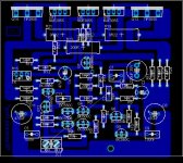
Attached is the schematic and layout.
Thanks for your valuable feedback. Changes are made accordingly:
1) Two-pole compensation out, buffered miller compensation added.
2) seperate gnd for decoupling caps (GND) and input+feedback+R6 (SGND).
3) zobel will be added at the speaker out binding post later if needed.
Pls note that in the drawing, MJE3055/2955 and TIP3055/2955 will be replace with MJE15030/15031 and MJL21193/21194 in actual implementation cos' can't find the library and the footprint is the same.
MikeB,
Can you explain why the offset will be high without input cap? Can you recommend what transistor to use in place of Q6,7,9?
Attached is the schematic and layout.
Attachments
Hi,
I would keep the Zobel/Thiel network on the output terminals.
Self tried to modify his ccs for the VAS & LTP to improve the asymetric slew rate and failed. His conclusion just stopped short of recommending separate ccs for both. I recommend two separate ccs for these stages. Each ccs can still share the decoupled supply. R6 should return to power ground not signal ground.
The rail decoupling should work at 100r/470uF you have shown 50r/470uF (the heat dissipation of one resistor should easily cope with the low level stages)
How about adding in an RF input filter? Set the series input resistor to match R7.
Richieboy,
FYI, I'm just browsing through Douglas book and are still reading it. In the mean time, hope you guys can help me through and give your suggestion.
Andrew,
What would be the optimum -3dB point for the low pass filter. My calculation show that 100R give 3.3Hz, while 50R give 6.8Hz. Would this matter?
I suppose Q7 is the current source for VAS, while Q6 is for LTP. May be I miss out something.
Do I need to add shunt a capacitor to the input to form RF filter with input series resistor?
BTW, do you forsee any hum noise in this layout? and can I use MJE15030/15031 and MJL21193/21194? ANy problem with this? If not I'll continue to build this up.
Thanks.
Hi,
yes a shunt cap and series resistor for the rf input filter. Try 680r & 1nF. Put in the series resistor AFTER the input impedance setting resistor. i.e. input terminal, shunt resistor(2M2), series cap(10uF or two 22uF back to back//1uF film), shunt resistor(10k), series resistor(680r), shunt cap(1nF or less), input transistor.
The NFB & PSU time constants should be similar to the decouple, so your 100r/470uF at 3Hz is OK. Personally I would leave room for 1000uF electro//100uF lesr//1uF film//10nF low inductance film//100pF ceramic and maybe 150r to give 150mS RC. If you decide to add an input dc blocking cap the RC should give a higher frequency than all three of the former filters or put another way each of the PSU, NFB and Decouple filters should have a larger RC than the input filter.
The VAS ccs is tapping the base signal from the LTP active ccs. It is outside the control loop. Self swapped these around to try to solve his circuit problems and failed to find a good solution. He appeared to be trying a save one transistor at any cost and as I said he did not suggest the obvious:- put in two separate ccs to LTP & VAS.
Regarding hum. I suggest following Self's advice on signal and dirty (power) grounds to the letter. Also read Leach for a slightly different grounding topology but still separate clean and dirty grounds. Note Zobel (Thiel), speaker, PSU, relays, chassis, mains safety earth and decoupling are all treated as being dirty returns. I had to read these and a few others many times before the philosophy finally sunk in.
With bipolar devices, the input impedance influence on distorsion is the object of an article from D. Self :
"Power amplifier input current and their troubles"
Doug Self, Electronics World, May 2003, p53
What does he say ?
The blameless amplifier must be driven from low impedances sources (50 Ohm). If driven form a 2.2 kOhm, distorsion increases by about 3 dB. For volume control, one needs a buffer after the pot, or an active circuit such as provided in his preamp. A partial solution is to cascode the long tail pair CCS of the input stage. The values Self uses for the input filter gives a very high frequency turnover : 50 Ohm and 1 nF.
I built my Self amp about ten years ago. There was no RF filter nor low value resistor in series with the input and I've never had problems with interferences.
I think that replacing the simple differential pair with a CFP pair should have two advantages : a better linearity and the avoidance of the need of a low source impedance, the input impedance of the input stage becoming very high.
Of course, an input coupling capacitor is needed to avoid any DC problems at the output. If nothing else is at hand, you can use electrolytics, + to the input PNP bases which are slighly positive. Bipolar capacitors are considered to be better and still occupy low room on the board. Add a high value resistor (100 kOhm - 1 Mohm) at the source side to discharge this capacitor. While experiemtning, I've blown up one of my amp because the lack of this resistor (there was no plan for it on my original boards from Signal Transfer) .
As said by AndrewT, the Self's advices for ground schemes give a very efficient philosphy to avoid hums. Just through short emails, I've helped some guys to resolve hum problems.
~~~~~~~~ Forr
§§§
Ipanema said:and can I use MJE15030/15031 and MJL21193/21194? ANy problem with this? If not I'll continue to build this up.
Thanks.
Hi !
I don't see prolems using these transistors, these are quite decent ones.
But, your choice for q7/q9 with bc550/560 is "bad". These have max
rating of 45v, this limits you to supply of max +/- 22v, above this supplyvoltage
you exceed the maxrating when amp goes to full swing.
If you want to keep to92 transistors, at least change them to mpsa41/42
or 2n5551/5401. (or others with high max-vce)
Mike
forr said:
Beware that the two pole compensation can lead to instabilities............
Only if you don't know how to apply it....
- Status
- This old topic is closed. If you want to reopen this topic, contact a moderator using the "Report Post" button.
- Home
- Amplifiers
- Solid State
- Blameless Amp layout