The hand-drawings of Nelson Pass hasn't stop inspiring people. The patent #3,995,228 has given birth to Hawksford Error Correction and NP-PMA Error Correction.
In the discussion on "Back EMF" (IF this speaker back-EMF existed AT ALL), the Hawksford type will be weak in this situation. It will convert the distortion of loudspeaker's back EMF to higher orders one (with smaller level, offcourse), because in Hawksford EC, the EC connects the speaker directly to the bases of the EC, any back EMF will be magnified because they are entering base(s).
NP-PMA error correction is much better facing back-EMF, because the EC transistors are operated in common base mode.
This time I'm inspired by patent #4,107,619.
In Error Correction cct's, there are 2 loops, one is the major audio loop and the 2nd is the smaller EC loop. Usually this EC loop is placed at the output stage.
Looking at the fig2 of this patent http://www.diyaudio.com/forums/attachment.php?s=&postid=698322&stamp=1123354150. It has the main audio loop around device 51, and smaller current loop around device 59.
Then NP gives me this post http://www.diyaudio.com/forums/showthread.php?postid=698475#post698475. He is saying that the whole concept can be made by a much simpler way, and he is right
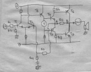
Then I draw this (attachment). At a glance, it seems nothing special, it is ordinary CFP output stage. But I think it works quite differently, it has EC loop around T4,T5,T6,T7,R5,R6,R7.
The main audio loop takes feedback from point A, it is not directly to the speaker node, but bridged by R5. I think about 10ohm for R5 and 100ohm for R6+R7.
The whole audio loop will determine the condition on point A, not the speaker node (point B).
If there is any voltage imbalance in R5, it will makes T6/T7 gives current until voltage A=B again.
For example : A is more positive from B. The current will be flowing from A to B. This means, the same current will be flowing in R6, since T4 is common base transistor for this case. The rising voltage in R6 (10x voltage rise in R5, 100ohm/10ohm), will be activating T6 to give current to point B until A=B=balanced condition.
The "CFP like" output stage is actually having local EC loop, without affecting the main loop
Another interesting properties is the feedback take point is separated by R5 value to the speaker, in this example is by 10ohm resistor. I hope any nonlinearity caused by loudspeaker back EMF (it it existed) will be taken care by the local EC loop on the output stage, not entering the differential, because the feedback node is from point A.
I have 2 questions.
-Is my thinking above works AT ALL?
-If it works, what is the output impedance of the whole system? Is it 10ohm output impedance (since the feedback take point is 10ohm away from the speaker)?
In the discussion on "Back EMF" (IF this speaker back-EMF existed AT ALL), the Hawksford type will be weak in this situation. It will convert the distortion of loudspeaker's back EMF to higher orders one (with smaller level, offcourse), because in Hawksford EC, the EC connects the speaker directly to the bases of the EC, any back EMF will be magnified because they are entering base(s).
NP-PMA error correction is much better facing back-EMF, because the EC transistors are operated in common base mode.
This time I'm inspired by patent #4,107,619.
In Error Correction cct's, there are 2 loops, one is the major audio loop and the 2nd is the smaller EC loop. Usually this EC loop is placed at the output stage.
Looking at the fig2 of this patent http://www.diyaudio.com/forums/attachment.php?s=&postid=698322&stamp=1123354150. It has the main audio loop around device 51, and smaller current loop around device 59.
Then NP gives me this post http://www.diyaudio.com/forums/showthread.php?postid=698475#post698475. He is saying that the whole concept can be made by a much simpler way, and he is right
Then I draw this (attachment). At a glance, it seems nothing special, it is ordinary CFP output stage. But I think it works quite differently, it has EC loop around T4,T5,T6,T7,R5,R6,R7.
The main audio loop takes feedback from point A, it is not directly to the speaker node, but bridged by R5. I think about 10ohm for R5 and 100ohm for R6+R7.
The whole audio loop will determine the condition on point A, not the speaker node (point B).
If there is any voltage imbalance in R5, it will makes T6/T7 gives current until voltage A=B again.
For example : A is more positive from B. The current will be flowing from A to B. This means, the same current will be flowing in R6, since T4 is common base transistor for this case. The rising voltage in R6 (10x voltage rise in R5, 100ohm/10ohm), will be activating T6 to give current to point B until A=B=balanced condition.
The "CFP like" output stage is actually having local EC loop, without affecting the main loop
Another interesting properties is the feedback take point is separated by R5 value to the speaker, in this example is by 10ohm resistor. I hope any nonlinearity caused by loudspeaker back EMF (it it existed) will be taken care by the local EC loop on the output stage, not entering the differential, because the feedback node is from point A.
I have 2 questions.
-Is my thinking above works AT ALL?
-If it works, what is the output impedance of the whole system? Is it 10ohm output impedance (since the feedback take point is 10ohm away from the speaker)?
Attachments
Hi, EVA,
Aha, I see the difference in our point of view. I remember somewhere you said that the whole feedback amp is an EC itself, why bother making the so called "EC"? You're right here, the feedback system is an "EC" itself.
If I wanted that the main loop fix it, I would take the feedback point from B, and R5 will have to dissappear.
I have tought that not everybody will agree with the basic concept itself.
Anyway,EVA, do you know what is the output impedance of the idea? I don't know how to calculate output impedance from a schematic.
Aha, I see the difference in our point of view. I remember somewhere you said that the whole feedback amp is an EC itself, why bother making the so called "EC"? You're right here, the feedback system is an "EC" itself.
This is exactly what I wanted. The feedback of the main loop is taken from point A, and if the speaker is giving any non-balance in A-B (R5), it will be corrected by the "CFP" local loop, not entering the differential (main global loop), because if it is entering the global loop, it will be transformed to higher order distortions.that feedback has no chance to correct.
If I wanted that the main loop fix it, I would take the feedback point from B, and R5 will have to dissappear.
I have tought that not everybody will agree with the basic concept itself.
Anyway,EVA, do you know what is the output impedance of the idea? I don't know how to calculate output impedance from a schematic.
It's hard to estimate output impedances, but you can put upper and/or lower limits to them very quickly.
For your circuit, output impedance won't be smaller than R5 divided by the instantaneous current gain of Q6 or Q7 depending on wich one is conducting.
Note that this current gain changes with frequency and with collector current, so it's a potential source of distortion (that neither the main loop nor the CFP loop can't attenuate).
I think that you are overlooking the effects of base currents and transistor non-linearities, while error correction is based just in the opposite practice.
David,
Just for the record, there are many error correction schemes around, but the Hawksford one is a very specific one. It does return the error to the correction point in exactly the correct amount to cancel it. Make it larger or smaller and you are back at some form of feedback (even if it is called error correction). The difference is that with fb, the larger the loop gain, the lower the final error or distortion. In the Hawksford case, lower or higher fb will increase the error. Only at the precise point where the correction factor is exactly one will there be a minimum of error. The other schemes you mention in your first post are NOT Hawksford error correction. PMA's design is error correction, but NOT Hawksford EC. NP's patent did NOT lead to Hawksford EC because it is something else. Reading Hawksford paper will make it clear.
Jan Didden
Two member said that I'm drawing CFP, maybe that is what I do Reinventing the wheel one more time.
Funny thing, is, that I got the final shape of CFP is from step-by-step thinking, resulting the same CFP. I'm not thinking at all at first to draw CFP. That's just what it looks like in the end.
At the process, I also think about "current drive" effect of R5 operation, I tought waw, I draw something here.
Janneman should be smiling at me now. In the "black box" approach that he likes, this is a joke. If I want to go from LA to New York, I can go straight from LA directly to NY, I also can go from LA to Alaska to London to Paris and end up in the same NY, Janneman's black box doesn't care, as long as I started in LA and finished in NY, that's it. If you go circling around the world first, it is the dumb of me.
At least, I learn what is the power burried inside the simple CFP
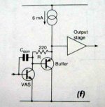
I think I'm not alone in "inventing the wheel". Douglas Self is also doing the same "circling around the world". You don't believe me? Look at his book about the "VAS OPERATION" chapter. It is on page 78 in my book (first edition).
In figure 4.17, he draws 6 variations of VAS. The interesting one is the (f) one. He said this is "Alternative buffering, bootstrapping VAS load R" Complicated, eh......
In the explenation he wrote this :
Reading the explenation is so complex. What does he draw? Look at the attachment.
Why don't he just say 2 words : "CFP VAS"?
Reinventing the wheel one more time. Funny thing, is, that I got the final shape of CFP is from step-by-step thinking, resulting the same CFP. I'm not thinking at all at first to draw CFP. That's just what it looks like in the end.
At the process, I also think about "current drive" effect of R5 operation, I tought waw, I draw something here.
Janneman should be smiling at me now.
In the "black box" approach that he likes, this is a joke. If I want to go from LA to New York, I can go straight from LA directly to NY, I also can go from LA to Alaska to London to Paris and end up in the same NY, Janneman's black box doesn't care, as long as I started in LA and finished in NY, that's it. If you go circling around the world first, it is the dumb of me. At least, I learn what is the power burried inside the simple CFP
I think I'm not alone in "inventing the wheel". Douglas Self is also doing the same "circling around the world". You don't believe me? Look at his book about the "VAS OPERATION" chapter. It is on page 78 in my book (first edition).
In figure 4.17, he draws 6 variations of VAS. The interesting one is the (f) one. He said this is "Alternative buffering, bootstrapping VAS load R" Complicated, eh......
In the explenation he wrote this :
A less well known but more dependable form of bootstrapping is available if the amplifier incorporates a unity-gain buffer between the VAS collector and the output stage, this is shown in Figure 4.17(f), where RC is the collector load, defining the VAS collector current by establishing the VBE of the buffer transistor across itself. This is constant, and RC is therefore bootstrapped and appears to the VAS collector as a constant-current source. In this sort of topology, a VAS current of 3mA is quite sufficient, compared with the 6mA standing current in the buffer stage. The VAS would infact work well with lower collector currents down to 1mA, but this tends to compromise linearity at the high-frequency, high-voltage corner of the operating envelope, as the VAS collector current is the only source for driving current into Cdom
Reading the explenation is so complex. What does he draw? Look at the attachment.
Why don't he just say 2 words : "CFP VAS"?
Attachments
[snip]Reading the explenation is so complex. What does he draw? Look at the attachment.
Why don't he just say 2 words : "CFP VAS"? [/B]
Would you buy a book with just two pages?
Jan Didden
lumanauw said:[snip]I think I'm not alone in "inventing the wheel". Douglas Self is also doing the same "circling around the world". You don't believe me? Look at his book about the "VAS OPERATION" chapter. It is on page 78 in my book (first edition).
[snip]
D Self is very good at tying together known things from very diverse sources and putting it in context in a single book. I don't think he invented anything.
Jan Didden
lumanauw said:Two member said that I'm drawing CFP, maybe that is what I do
Funny thing, is, that I got the final shape of CFP is from step-by-step thinking, resulting the same CFP. I'm not thinking at all at first to draw CFP. That's just what it looks like in the end.[snip]
Congratulations! You think just like the big guys do.! (And i mean that!).
Jan Didden
lumanauw said:[snip]Janneman should be smiling at me now.
Well, the analogy is not quite right. You can have two black boxes that seen and measured from the outside are the same. That does not mean they actually are. One can be very simple and "smart" the other can be very complex and difficult. But you can't know which is which.
In your travel black box example, seen from outside the box they both provide a trip from LA to NY, but one does it much better. Yet, in the analogy, seen from the outside, they do the same thing: take you from LA to NY.
Really, David, the bb analogy is such a powerfull paradigm in analysing complex situations, denying yourself that only makes it harder.
Jan Didden

Why don't he just say 2 words : "CFP VAS"?
Because it's not a CFP (although the transistors are connected in the same way). The only local feed path is Cdom. R loads the VAS stage with a constant current and the buffer acts like it is named: as buffer. There is no return path to the VAS. In a CFP the emitter of the first stage is coupled back from the collector of the second stage giving 100% voltage feedback. Here the REFERENCE for the emitter of Q1 and the collector of Q2 is V- so there is no return path available. No feedback = no CFP. So I would not call this CFP VAS
Hi, Bocka,
I think about the feedback point of the global feedback is taken in point A, and speaker node is point B, they are apart by R5 (I'm thinking about 10ohm for R5). EVA pointed that it has 2 loops like I tought.
Do I make EC or just making CFP? From your criterion, it does have 100% voltage feedback (but it is doing so not like ordinary "CFP" which is emitor of the driver and collector of the driven is tied together without R5, but with current drive of R5, T6 and T7 will always naturally try make voltage A=B), does this makes the idea is just a CFP?
This is very interesting, especially this partBecause it's not a CFP (although the transistors are connected in the same way). The only local feed path is Cdom. R loads the VAS stage with a constant current and the buffer acts like it is named: as buffer. There is no return path to the VAS. In a CFP the emitter of the first stage is coupled back from the collector of the second stage giving 100% voltage feedback. Here the REFERENCE for the emitter of Q1 and the collector of Q2 is V- so there is no return path available. No feedback = no CFP. So I would not call this CFP VAS
It is a real honour if you give me your opinion about what I draw in post #1. What is it?Because it's not a CFP (although the transistors are connected in the same way).
I think about the feedback point of the global feedback is taken in point A, and speaker node is point B, they are apart by R5 (I'm thinking about 10ohm for R5). EVA pointed that it has 2 loops like I tought.
Do I make EC or just making CFP? From your criterion, it does have 100% voltage feedback (but it is doing so not like ordinary "CFP" which is emitor of the driver and collector of the driven is tied together without R5, but with current drive of R5, T6 and T7 will always naturally try make voltage A=B), does this makes the idea is just a CFP?
Hi, PMA,
I'm confused At first you said this :
Then you said this :
Again, am I drawing EC in post #1 or just CFP?
I'm confused
At first you said this :
Yes, this is a traditional CFP output stage, I have it also in one of my amplifiers, operating in class A. But with different bias circuit.
Then you said this :
How about R5? In case of R5 approaching to zero, we have a standard CFP output stage.
Again, am I drawing EC in post #1 or just CFP?
I have overlooked the R5 firstly. You can see output CFP stage here:
http://www.pha.inecnet.cz/macura/pma1.gif
http://www.pha.inecnet.cz/macura/pma1.gif
The global feedback is only controlling voltage at point A, it doesn't care about point B.
T6 and T7 works by giving or sucking current so point B will have the same voltage as point A. T6 and T7 doesn't care about the global feedback (what voltage in A should be), it only "views" the condition of point A and B , by giving or sucking current until A=B.
T6 and T7 works by giving or sucking current so point B will have the same voltage as point A. T6 and T7 doesn't care about the global feedback (what voltage in A should be), it only "views" the condition of point A and B , by giving or sucking current until A=B.
- Status
- This old topic is closed. If you want to reopen this topic, contact a moderator using the "Report Post" button.
- Home
- Amplifiers
- Solid State
- Error Correction Idea