
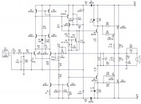


A few comments: Blue LEDs are not the best to use for voltage references, since they are more noisy than other colours.
Your frequency compensation is quite complex. Does it have to be like that? The more complex it is, the more likely it is that the sim will differ from reality, requiring more work prototyping. Using an output stage with gain will make it that much more difficult.
The 0.22 resistors are on the wrong side of the MOSFETs. They should be in the source.
The 0.22 resistors are on the wrong side of the MOSFETs

The more complex it is, the more likely it is that the sim will differ from reality, requiring more work prototyping. Using an output stage with gain will make it that much more difficult.
I think that you'll get also problems with thermal stability because the thermal voltage tracking of your Vbe multiplier is multiplied by 10 (R4/R18) which then controls the Vgs of your MOSFETs.
R29 and C16 makes more sence in the collectors of Q16 and Q17 anthough i would recalculate the values
Thanks for yor reply.
I didn't know for the blue LED noisyness. The upper one is for a second stage cascode voltage reference only. I can be substituted with other type of LED or anything else then. For the other one - D7, it can be green or red or anything, just R1 and R7 must be recalculated, so thanks for sharing your knowledge.
About the frequency compensation: r12, r13, r14,c6 and c7 at the input are only to prevent RFI. They can be replaced with ordinary input filter - one capacitor in series with the input and one resistor for input impedance, so they are not critical. I've experinted with them and their impact on the frequency and phase characteristic is very little. C6 especially can be removed without any harm. R29 and c16 in the LTP too are not critical even with double values (all combinations) the impact is not so great. There is very little voltage amplification in this stage, so they are there only to prevent oscillations, but I think they are pretty ordynary approach. I've seen many amps with such compensation, and some of them are pretty good ones.
About c12 - again pretty standard approach. R29, C16 and c12 can be removed too, provided that the miller capacitor C5 is changed to 80-100pf, but this would affect the slew rate.
The amplification in driver stage is only to allow the output swing to be comparable with a BJT amp. This maybe will add some instability, I absolutely agree with you. Thats why the above frequency compensation is choosed. C11 cap too are placed for this reason - to swamp the frequency response above the audible frequencyes.
The output filter network id pretty standard i thing.
Why do you thing the 0.22ohm resistors are on the wrong side? Please explain this for me. They are only for better current sharing of the output MOSFETS? If they are properly matched I don't see a problem.
I am not very experienced in making audio amps, so all the above may be wrong. I will be glad to see any comment.
Thanks again.
About R29 and C16 - absolutely agree - Q16 and Q17 are there to supply a constant voltage to Q1 and Q2, so the voltage swing will be very small there (considering high gain of Q16 and Q17). Considering the second stage is BJT without emiter resistor on Q7, there will be also small voltage swing on collectors of Q4 and Q5, but larger then on the emiters. Am I right?
I'll try to recalculate them and put them on the right place and see what happens.
btw, Q16 and Q17 are there only because I wanted to use a transistors with high gain in input stage. Same reason for second stage cascode. This I guess will compensate for cheap output devices (IRF540/9540) nonlinearity. Am I right on this also?
What would you suggest for thermal stability? Q18 will be mounted on the output device's heatsink. Wouldn't this compensate a little?
P.S: Excuse my bad english - need a little more practice.")
I'll try to recalculate them and put them on the right place and see what happens.
btw, Q16 and Q17 are there only because I wanted to use a transistors with high gain in input stage. Same reason for second stage cascode. This I guess will compensate for cheap output devices (IRF540/9540) nonlinearity. Am I right on this also?
What would you suggest for thermal stability? Q18 will be mounted on the output device's heatsink. Wouldn't this compensate a little?
P.S: Excuse my bad english - need a little more practice.
Other comments have more substance than mine, but here goes:
Your bypass caps use the same ground network as the signal return. This is functional but also a way to get noise from the rails into the input signal. I suggest you make there two separate ground paths the meet off-board at a "star point.
I believe that just as BJT emiiter-follower out put stages are the more stable configuration, so with MOSFETs a source-follower is more stable. Since this is your first amp I suggest sticking with a follower configuration. If want to try something different get a stable, functioning, good sounding EF/SF design built (not just sim'd) first. Then using that as a base, reconfigure the output section as you prefer. I predict you will find getting the more "exotic" configuration (meritorios though it may be) stable and functional is a major project just on it's own.
sam9, I know for the grounds. This is just in the simulator, because it doesn't support different grounds, and even if it does, it is pointless to do it in simulator, because there will not be any difference I think.
I agree that source follower is more stable, no doubt about that. I just want to experiment. I will try to make the PCBs in a way to be able to make both output configurations and experiment with them.
I think that the source follower with HITACHI lateral MOSFETs will sound great - absolutely, But what I want to achieve is a good amp with more cheap components. In my country the HITACHI devices are up to 10 times more expensive then IRFs. And if I make source follower with IRFs, the output swing will be about 5-6V less then with HITACHI laterals - This is exactly what I am trying to avoid using this configuration for output stage. This is why there is a little amplification in the output stage - i've tried to make that amplification as small as possible - just enough to compensate for the voltage, needed to drive the MOSFETs.
This can be achieved of course using a bit higher voltage power supply for input and driver stage, but this is not an elegant enough solution for me, dont you think?
Specifically I am referring to R29/C16 and C5. A capacitor in the position of C5 is what is usually used to provide dominant pole compensation: It rolls off the frequency response at 6dB/octave so that it falls below 0 before the phase shift reaches 180 degrees, ensuring stability. C16 adds an additional 6dB/octave at some frequency, plus extra phase shift. R29 stops that extra roll-off at some point.sparkybg said:About the frequency compensation...
These poles and zeroes need to be positioned carefully so that the frequency response rolls off smoothly. Sims won't always be very accurate in this case. If you get it right you can end up with an amp that is faster than normal, but since you're not yet experienced, I would recommend sticking with only C5, which may need to be a little bigger.
I like output stages with gain - as you say, they increase output swing, as well as increasing slew rate and potentially lowering distortion slightly, but they add more phase shift, which makes stability more difficult to obtain. Go ahead and try it if you want; If it works then great, if not then you gain experiencesparkybg said:The amplification in driver stage is only to allow the output swing to be comparable with a BJT amp. This maybe will add some instability, I absolutely agree with you. Thats why the above frequency compensation is choosed. C11 cap too are placed for this reason - to swamp the frequency response above the audible frequencyes...
Those resistors provide current feedback when in the sources: As current through the FETs increases, so the voltage across the resistors increases. This decreases gate-source voltage of the FETs, reducing the current through them. If the resistors are in the drains, then they have no particular effect, since the current thought the FETs depends little on the source voltage.sparkybg said:...Why do you thing the 0.22ohm resistors are on the wrong side? Please explain this for me. They are only for better current sharing of the output MOSFETS? If they are properly matched I don't see a problem.
Even well-matched vertical MOSFETs should have source resistors due to their positive temperature coefficient, which will tend to channel more current through whichever one is warmest.
Very nice.
High feedback, probably too high (to my taste).
I would add some emitter resistors in input differential stage.
0.22 resistors are on the wrong side as mentioned before.
R29 and C16 are not only redundant, but may even become problemous- Q16, Q17 common base stage won't like anything capacitive in emitters.
Running +-48V rails is preey close to irf540 max. VDS- beware.
You can also try some smaller gate stoppers like 150 ohms, your output stage is really slow with 470 ohms.
just suggestions
regards

 Thanks guyz. You are very helpfull.
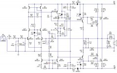
 Below is the updated version. Similar results on simulators.
- Changed position of 0.22ohm resistors.
- Changed position of R29 and C16. and recalculated.
- Added emmiter resistors in LTP.
- Blue LEDS changed to green and zener. Recalculated R1,R2 and R7
- Changed gate protection zeners from 8.2V to 9.1V.
Any other suggestions/comments?
Specificaly about thermal stability?
I know the gate resistors are large, but I will experiment when I make the amp. Maybe 270ohm is more suitable.
+-48 will be the absolute maximum for the supply - with minimum load and maximum line voltage (250V AC). This is just for testing to the limits. The IRF640/9640 would work for higher voltages, but i don't need more power than this. (100-150W on 4 ohm).
Attachments
Not sure if you have actually built on. MOSFET CFP output stages are a bitch to get to work. I have tried countless ones and few could work on the first try. And even that, a little bit of disturbances (like plugging / unplugging etc. will set them on fire).
Hope you have better luck. Otherwise, I would suggest EF output stages for MOSFETs.
Hope you have better luck. Otherwise, I would suggest EF output stages for MOSFETs.
Banned
Joined 2002
- Status
- This old topic is closed. If you want to reopen this topic, contact a moderator using the "Report Post" button.
- Home
- Amplifiers
- Solid State
- My 200W/4 class AB MOSFET amp.