Wait till we mods cut out some posts.Christer said:

Congrats on this nice group effort.
/Hugo
Upupa Epops said:Why do you make it by this way, you, guys from some of richiest country of world ? And in this time ?
Who, me? Not all of us are
 , not yet
Lukas
Upupa Epops said:Why do you make it by this way, you, guys from some of richiest country of world ? And in this time ?
Very simple, etching your own PCBs is a big part of the whole fun making electronics !

Mike

 Interesting look at this kind of "fun" from a completely different point...
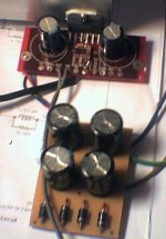
MikeB said:
Very simple, etching your own PCBs is a big part of the whole fun making electronics !
Mike
Michael,
let me respectfully disagree. All you get with "hand-made" PCB is unpredictable thickness of copper layer, possible hair-thin non-conductive gaps, unsticked copper pads after desoldering. "Hand-made" PCB is absolutely unsuitable for DIY work, as there is usually need to repair mistakes.
I would never have had the nerves to evaluate Symasym on hand-made PCB ....
Pavel
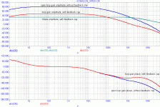
MikeB said:Pavel, you may explain which curve of the 3 phaseplots represents which node ?
Mike
Michael,
sure. Sorry for small delay, but I decided to prepare a new graph with standard feedback terminology included. Here it is, and I am sorry for my pencil-drawn graph shown before.
The graph attached shows contribution of the feedback capacitor as well.
Pavel.
Attachments
PMA said:
Michael,
let me respectfully disagree. All you get with "hand-made" PCB is unpredictable thickness of copper layer, possible hair-thin non-conductive gaps, unsticked copper pads after desoldering. "Hand-made" PCB is absolutely unsuitable for DIY work, as there is usually need to repair mistakes.
Pavel, i also respectfully disagree with you...
") Once you get this technique refined, the resulting PCBs are "perfect", not showing a single flaw. But it needs to be the photochemical process. I can show you a macrophoto of pcb this evening, no underetching, no holes, no varying thickness. Yes, desoldering can destroy them, but an industrial made, singlesided would show the same syptoms, it's the same material and process !
Once you get this technique refined, the resulting PCBs are "perfect", not showing a single flaw. But it needs to be the photochemical process. I can show you a macrophoto of pcb this evening, no underetching, no holes, no varying thickness. Yes, desoldering can destroy them, but an industrial made, singlesided would show the same syptoms, it's the same material and process !The advantage of diy-pcbs ? From printout to etched pcb, ~1hour + 1hour drilling.
But for doublesided PCB...

Mike
Michael,
OK . Our view is different, it does not matter at all.
I assume you've noticed that the PCB I used for symasym evaluation was double-sided, with the plated-through vias and solder mask.
During my professional carrier I went through all the steps of PCB design and production, and I would never return to home-made boards .
Pavel
OK
. Our view is different, it does not matter at all.I assume you've noticed that the PCB I used for symasym evaluation was double-sided, with the plated-through vias and solder mask.
During my professional carrier I went through all the steps of PCB design and production, and I would never return to home-made boards
.Pavel
All you get with "hand-made" PCB is unpredictable thickness of copper layer, possible hair-thin non-conductive gaps, unsticked copper pads after desoldering. "Hand-made" PCB is absolutely unsuitable for DIY work, as there is usually need to repair mistakes.
I would never have had the nerves to evaluate Symasym on hand-made PCB ....
Hi Pavel,
up to some years ago I did this for a long time, about 15 years or so. Worked fine, not only for audio boards but also for my first self build computer system

At the end of my self etching time I also did double sides PCBs. The limits I reached was about 15mil trace and gap. and 25mil for drills. I went away for this when I was able to use a PCB milling machine, but this wasn't much better, but saved me some time.
Nowadays I'm using PCB prototype services only, but I agree with Mike, etching PCBs is a lot of fun for DIY.
Hi bocka,
much of similar experience, I did my first uP system based on I8080 in the beginning of 1980 on 2-sided, non-plated-through vias, non-HAL PCB. But just in the middle of eighties I always used PCBs with plated-through vias, only solder mask was missing (I speak about uP and memory boards/.
Pavel
much of similar experience, I did my first uP system based on I8080 in the beginning of 1980 on 2-sided, non-plated-through vias, non-HAL PCB. But just in the middle of eighties I always used PCBs with plated-through vias, only solder mask was missing (I speak about uP and memory boards/.
Pavel
“"Hand-made" PCB is absolutely unsuitable for DIY work…”
Begs the question, what kind of work are they suitable for, then?
I’d like all my pcb’s to be double sided PTH, solder resist coated and silk screened, but I can’t do that at home (at least, not without an inordinate amount of trouble-but if I could, I’d go surface mount), and getting the artwork fabricated onto FR4 at a pcb house can be expensive for a few off, which could be wasted if the design, or my execution of it, doesn’t live up to expectations (or the hype!). For this forum, a group buy can be the answer, if it’s a popular design and your happy with the layout presented (and someone’s prepared to take it on).
Then again, it depends on what you mean by “hand made”. If Dalo pen drawn direct on copper clad, they usually look terrible. I’ve been making my own PCB’s for thirty-odd years, using liquid positive resist, litho photography, tape and pads, and latterly, CAD and ink jet for the artwork, building various amps and test gear, still in use, without too much of a problem. There’s usually something I don’t like about the original posted layout, (if indeed there is one) as this forum, ever so politely, often points out, so I’ll usually re-design it to my satisfaction. Then there is the advantage that you can incorporate features not in the original design, such as output protection in PA’s. Having done all that, if, after making it myself, it works as described, fine; if not, I’ve not lost much financially and gained even more experience as to how not to do it in future.
Anyway, for me, DIY means just that. I feel I have to contribute something original, otherwise I’ll just buy a kit and assemble it. There is an expression used in the PCB assembly industry-“all we make is soldered joints”. By designing and making my own PCB’s, I’d like to think I do more than that.
Brian.
Brian,
it is only up to you to make your decision (what kind of PCB to use).
I only spoke about pros and cons of both attitudes.
As almost everyone, I had also started as a DIYer when I had been 14 yrs, and of course went through different stages of PCB prepare and manufacturing.
I do not force anybody to use professional PCBs.
- Home
- Amplifiers
- Solid State
- Explendid amplifier designed by Michael Bittner, our MikeB