I've just built a new amp, and I'm getting some strange issues when adjusting the bias. I'm stumped if this is a real bias issue, or oscillation. I'll post some schematics later when I draw a new one.
I'm using a pair of 9V batteries connected to make +/-9V (18V) for testing the amp until I'm 100% sure I can connect it to the designed +/- 60V rails.
When I have the bias at minimum, I only measure less than 5mA of standby current which I know comes from my VAS and diff stages. The amp plays music fine, my offset is within 10mV and it sounds good, but I know it's class B with min bias, even though I can't hear the crossover distortion much if at all.
The problem comes when I raise my bias to try to run class AB. I raise it slowly until only about 10mA and then the amp starts pulling max current (1.6A from the 9V cells ) I can't adjust anywhere in between! Even stranger, if I have my bias adjusted just below around 9-10mA and start playing music, the current will sometimes switch to max current on its own
  , but if I have the bias down to minimum, I never get that problem.
Any recommendations would be helpful.
Thanks
I'm using a pair of 9V batteries connected to make +/-9V (18V) for testing the amp until I'm 100% sure I can connect it to the designed +/- 60V rails.
When I have the bias at minimum, I only measure less than 5mA of standby current which I know comes from my VAS and diff stages. The amp plays music fine, my offset is within 10mV and it sounds good, but I know it's class B with min bias, even though I can't hear the crossover distortion much if at all.
The problem comes when I raise my bias to try to run class AB. I raise it slowly until only about 10mA and then the amp starts pulling max current (1.6A from the 9V cells
) I can't adjust anywhere in between! Even stranger, if I have my bias adjusted just below around 9-10mA and start playing music, the current will sometimes switch to max current on its own , but if I have the bias down to minimum, I never get that problem. Any recommendations would be helpful.
Thanks
Thanks for the responses folks.
Now I'm sure it's oscillation, I'm looking for different ways to try to reduce it. Now this amp is being used for a subwoofer, but for testing it plays full range great. Since it's really only going to be for low frequencies, should I increase the 100pf caps?
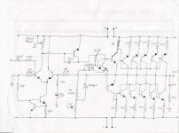
I've attached a Schematic
Uses MJL 4281 and 4302 for outputs with MJE15034 and 15035 drivers, all on heatsink. Also uses MJE15035 for VAS. Diff stage & CCS transistors use 2SC2632, 150V transistors.
The dual VBE multiplier transistors are because I have two seperate heatsinks and wanted temp compensation for both.
It's designed to have two separate powersupplies, so the vas and diff stage have their own power, but for testing with the batteries I connected the positives and negatives together, and all grounds go to one point on the PCB.
ANY tips on how to get rid of the oscillation would be greatly appreciated!
Thanks
Eworkshop1708
Now I'm sure it's oscillation, I'm looking for different ways to try to reduce it. Now this amp is being used for a subwoofer, but for testing it plays full range great. Since it's really only going to be for low frequencies, should I increase the 100pf caps?
I've attached a Schematic
Uses MJL 4281 and 4302 for outputs with MJE15034 and 15035 drivers, all on heatsink. Also uses MJE15035 for VAS. Diff stage & CCS transistors use 2SC2632, 150V transistors.
The dual VBE multiplier transistors are because I have two seperate heatsinks and wanted temp compensation for both.
It's designed to have two separate powersupplies, so the vas and diff stage have their own power, but for testing with the batteries I connected the positives and negatives together, and all grounds go to one point on the PCB.
ANY tips on how to get rid of the oscillation would be greatly appreciated!
Thanks
Eworkshop1708
Attachments
Can you measure frequency? If you DMM has a freq setting try looking at the output.
If it shows 100-500kHz, I would concentrate on the NFB network -- perhaps increasing the value of the Miller cap (200pF for starters).
If it shows MHz, I would suspect the CFB output as a place to look. I can't say much about taming the CFB configuration as frustration with them drove to EF. However, if confronted with this, I would start by removing all but one pair of output devices until I got that stable then add back pair one set at a time. Also I notice an absense of Rc resistors. My limited (non-) success with CFB suggests 0.47R improve the chances for stability.
Final idea, un-related (I think) to the above -- it's a good idea to keep a bit space between the IS&VAS on one hand and the output secion on the other. I also notice the absence of an output inductor. If you have one but it just doesn't appear on you schematic, don't let it gety near the input. It ain't called an inductor fer nuthin'.
If it shows 100-500kHz, I would concentrate on the NFB network -- perhaps increasing the value of the Miller cap (200pF for starters).
If it shows MHz, I would suspect the CFB output as a place to look. I can't say much about taming the CFB configuration as frustration with them drove to EF.
However, if confronted with this, I would start by removing all but one pair of output devices until I got that stable then add back pair one set at a time. Also I notice an absense of Rc resistors. My limited (non-) success with CFB suggests 0.47R improve the chances for stability.Final idea, un-related (I think) to the above -- it's a good idea to keep a bit space between the IS&VAS on one hand and the output secion on the other. I also notice the absence of an output inductor. If you have one but it just doesn't appear on you schematic, don't let it gety near the input. It ain't called an inductor fer nuthin'.
If I put a capacitor across the VBE transistor could that help stability?
My outputs and drivers and VBE multiplier transistors are all mounted to the heatsinks, all other components are on the PCB.
Also, I know my design doesn't have output resistors, I'm trying to achieve a low damping factor, and have as much current go to the speaker as possible. If I do end up needing to add output resistors, would some 10W 0.15 Ohm resistors be fine?
Would it do any good to add a resistor in the emitter leg of the VAS?
I'm also thinking of adding a 100pf cap on the base input of the CCS.
Would adding resistors to the base leads of the driver transistors also help?
Hi EW1708,
You have considerable output stage hf phase change in this topology. This is causing instability within the global NFB loop as you increase the gain/bandwidth product with increasing bias current. Even if you sort it at low voltage, it could return in a manner that will distort music as the output devices warm up when running with higher rails.
The compound output stage might appear ideal in isolation, but it introduces local stability issues when used like this. In a full range application you would need so much high frequency limiting to make it stable, that the performance could end up being inferior, but you might be okay for the sub-bass application.
Modern devices also need much more output shunting at hf than they did years ago, and with ten high power output devices you could take the R down to one ohm; better still when driving a woofer, use multiple R-Cs.
Cheers ......... Graham.
Thanks, I'll try those things to see what helps.
But is it really necessary to go with an EF output instead of CFP?
Also, why would the CFP outputs themselves have bad phase change at HF? Could it be the 5 inch long wires used to connect the PCB to the output stage be having too much inductance? Or is it just the nature of the topology?
I'll try to make the CFP work first, but if I still have trouble, I can re wire the outputs and drivers to make an EF output stage.
I know my design doesn't have output resistors, I'm trying to achieve a low damping factor
Even with a bunch og 0.47R (or 1R for that matter) Rc resistors your output impedance will be pretty low. Low enough to have a high damping factor.
Not if if you get the CFP working. BTW if you get it working, one of it's advantages is that the Vbe multiplier doesn't need to be on the heatsink with the output devices. Infact that may not be desirable. Same with the drivers. Consider using small board level sinks for the drivers and piggyback the Vbe multiplier to one of them.But is it really necessary to go with an EF output instead of CFP?
Don't know about phase change, but the output devices and the drivers are in a very tight local feed back loop. Theat's the cause of both the benefits and the problems. If the problem is local to the CFB the oscilation freq, if you can determine it, will probably be in MHz whereas if it is in the global NFB it will likely be much lower. At least that's the way it has worked for me.Also, why would the CFP outputs themselves have bad phase change at HF?
You really DO need the emitter resistors or the CFPs get unstable. Also, thermally, the transistors that must be coupled are the front end of the CFP and your Vbe multiplier. Coupling the output transistors may be a problem but if they have emitter resistros, this is unlikely, as they will be locally linearised. CFPs have a notable drawback when used with multiple output transistors in parallel, that yoo need emitter resistors in every one of the output transistors, and then common 'effective emitter resistors' for the first BJT in the CFP, for everything to be rock solid. Ergo, you get two places ehre you get power rail loss. When using CFPs, think of them as one transistor, with the polarity of the input one in the CFP. Also, keep in mind that the CFP is not the lowest rail loss output. It is impossible for the CFP to drive the output transistor to saturation, which means you have one Vbe of voltage drop on the CFP what ever you do. This is because the first transistor in the CFP can only connect the collector and base of the second transistor together, which is exactly the threshold of saturation for it, but no saturation occurs at all. Depending on the application, this can be good or bad - for instance, this is why you rarely see MOSFET in classic CFP connection - you get several V of loss. Unlike EF, you cannot cure this by giving the preceeding stages higher power supply rails.
You also do not need two transistors in the Vbe multiplier even if your outputs are spread across two heatsinks. Why? Consider Kirchof's laws - if one heatsink gets warmer, and at same Vbias passes more current, in order for the net DC at the output to stay the same, so do all the transistors on the other heatsink. Since both power rails are the same voltage, the other heatsink will then heat up as well. The only way you could get different currents in the two banks of transistors would be if you had a rectifying load, or a net DC voltage at the output, and you have neither (unless there is a serious fault, in which case bias current stability is the least of your worries.
What you may get with only one Vbe multiplier on one transistor, is a slightly different variation of bias current with temperature, but no instability.
Normally, in your configuration, the first ('driver') transistor in the CFP would be on board and the Vbe multiplier thermally coupled to IT, NOT the power transistors on the heatsink. In such a configuration, for outboard mounted power transistors, each of them needs a small base damper resistor, in series with the base (usually it's on the order of 4.7 - 15 ohms). Increasing bias increases the gain bandwidth product of the power transistors quite rapidly, and without a base damper, with a signifficant length of wire on the base and emitter, they can self-oscillate.
If the Vbe multiplier is outboard mounted, then you MUST use a capacitor in parallel ON BOARD to prevent audio currents going through long wires to it. At the very least, use a twisted pair of wires to get from the board to the Vbe multiplier in order to reduce the wiring inductance, not doing so is an invitation for oscillation problems.
An emitter resistor in the VAS transistor will linearise it's voltage gain - which in this application is really not necessary because the VAS is current driven. The total open loop gain of the amplifier will be lower, but wether this is good or bad depends heavily on many things, not the least of being what order of magnitude of an emitter resistor are we talking about. Emitter degeneration of the VAS gives it a better defind input impedance, but requires a voltage swing from the LTP. It is sometimes used to limit the maximum sink current of the VAS, to prevent oversaturation of one half of the output stage on clipping, though there are better ways to do this.
Thanks for the responses!
OK, I'm going to try a few things:
Add some output resistors.
Change zobel to 1 ohm, and/or zobel cap to 0.2uf
Add 1uf cap across VBE multiplier to see if it makes a difference.
Add 3.3 or 4.7 ohm resistors in series with the bases of my drivers and connect 100pf caps from the driver base leads to Ground. I figured the resistor + the 100pf cap may hopefully bypass any real high frequencies away from entering the output. I'll also try putting base resistors on the power transistors too.
I'll keep you folks posted!
Rather similar topology to Elliot's P3A....
You really do need emitter resistors or things go tits up. I decided CFP's are too much hassle and went for the Triple Darlington output. With that many power devices being run from one driver, you might be best with small (say 10 ohm) resistors in the power devices base (one per device)
You really do need emitter resistors or things go tits up. I decided CFP's are too much hassle and went for the Triple Darlington output. With that many power devices being run from one driver, you might be best with small (say 10 ohm) resistors in the power devices base (one per device)
Ilimzm & jaycee,
As point of clarity do you mean "emitter resistors" or "Collector resistors"? The output is taken off the collectors and he already has emitter resistors (0.13R).
As point of clarity do you mean "emitter resistors" or "Collector resistors"? The output is taken off the collectors and he already has emitter resistors (0.13R).
But when and if they do work the results can be rather nice.CFP is one of those things that look great in theory but hard to get to work in reality.
Hi Eworkshop.
Do you have a phobia of emitter resistors - because you have none, and you need some. You need 2x100 ohms in the diff's pair, 33 ohms in the Vas emitter (and 2 series diodes from +Vs to driver base), and 5.6 ohms in the driver emitters.
That should do it. Check for clean clipping.
You realise also that the closed loop gain is very high at 69, some 3 times normal.
Good luck.
Greg
Speaking of adding resistors..........
Instead of having a base resistor for each power device, couldn't I just have one base resistor that feeds the base leads of the power transistors since they are connected together?
Also, since the collectors are all connected, instead of using several "emitter" resistors to each collector of the outputs, couldn't I just use one for each set of 5 transistors?
I've seen other CFP circuits with just one pair of output resistors before that have had paralleled transistors, but of course each emitter also had a resistor to even out the load just like mine.
amplifierguru said:Hi Eworkshop.
Do you have a phobia of emitter resistors - because you have none, and you need some. You need 2x100 ohms in the diff's pair, 33 ohms in the Vas emitter (and 2 series diodes from +Vs to driver base), and 5.6 ohms in the driver emitters.
That should do it. Check for clean clipping.
You realise also that the closed loop gain is very high at 69, some 3 times normal.
Good luck.
Greg
What are the diodes for, to keep the input drive voltage from exceeding the rails?
Is it bad to have a high gain? If it is too high I can raise the value of the 930 ohm resistor.
Also I'm going add a resistor to the emitter of the VAS, and drivers, but regarding 100 ohm resistors for the Diff stage, I thought that the purpose of using resistors in the diff stage was to reduce offset. My offset is adjustable, so I didn't think they were necessary when I built the amp, but if they can help stabilize the amp, I may also try that.
- Status
- This old topic is closed. If you want to reopen this topic, contact a moderator using the "Report Post" button.
- Home
- Amplifiers
- Solid State
- Strange biasing issue when adjusting VBE