Just some really quick thoughts....
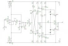
It looks to me like your volume control isnt wired correctly. It shorts the output of the opamp.
Your Q1 to Q4 looks interesting. I never see a topology like that. Do you have a reference about it?
I know that some mosfet amps have just a resistor for bias but they really do have +ve temp coeff at low current. You probably do need a Vbe multiplier there.
You have lots of stages. Each stage contributes at least a HF pole which means your HF response gets really complicated. This can make an amp hard to stabilise but I dont know for sure.
Doug
And one more, very simple amp.
An externally hosted image should be here but it was not working when we last tested it.
Attachments
Hallo vAD
I advise to change the 'diamond' Q1-Q4. I mean to NOT connect collectors of previous stage with emitters of the next stage.
This may cause higher offset and power supply noise.
I would connect collectors dirctly with rails. Another things:
-I think you don't need R55/56
-if you modify diamond as I said probably you won't need offsset pot
-maybe higher idle current in driver stage?
-probably you will need frequency compensation: maybe a small (say:100p) capacitor from bias pot to the ground
-small resitor on q1/2 emitters would be a voltage devider to prevent next stage from working in class (a)b
overal it look pretty nice to me-topology is OK!!!
Your pot is wired wrong on the schematic, as it is shorting the output of the OPamp, wich will only start reducing the output from it when it starts clipping because it's overcurrent protection is activated. If you really need to use such a volume control, connect it after R35.
Otherwise, you have an extra Opamp stage which really doesn't do much (especially if it is a TL072, it's a bit difficult to see in the picture). However, since it is a FET input OPamp, your offset voltage will be largely dependant only on gain and input offset from your DC coupled source.
I can se you have read some of my musings on pairing HEXFETs originally designed for switching applications, and use a IRFP240 and 9140. However, with the source resistors 0.22 ohm, you will still run into bias current runaway unless bias is quite high (on the order of 300-500mA or more), so you may want to look into using a Vgs multiplier somewhere. With HEXFET, you would need quite large source resistances (ohms) to get them stable at low bias, which would at the very least waste a lot of power.
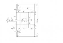
Regarding the other simple amp, the power supply generator for the OPamp seems a bit problematic to me, maybe a connection missing somewhere - the picture is fuzzy. You may want to try reducing to 16 colors and posting as GIF without reduction in size.
Otherwise, you have an extra Opamp stage which really doesn't do much (especially if it is a TL072, it's a bit difficult to see in the picture). However, since it is a FET input OPamp, your offset voltage will be largely dependant only on gain and input offset from your DC coupled source.
I can se you have read some of my musings on pairing HEXFETs originally designed for switching applications, and use a IRFP240 and 9140. However, with the source resistors 0.22 ohm, you will still run into bias current runaway unless bias is quite high (on the order of 300-500mA or more), so you may want to look into using a Vgs multiplier somewhere. With HEXFET, you would need quite large source resistances (ohms) to get them stable at low bias, which would at the very least waste a lot of power.
Regarding the other simple amp, the power supply generator for the OPamp seems a bit problematic to me, maybe a connection missing somewhere - the picture is fuzzy. You may want to try reducing to 16 colors and posting as GIF without reduction in size.
darkfenriz
Thank, I shall make your changes, but the circuit at present works, the truth while in a breadboard model.
Please. More precisely.
darkfenriz said:-small resitor on q1/2 emitters would be a voltage devider to prevent next stage from working in class (a)b
Thank, I shall make your changes, but the circuit at present works, the truth while in a breadboard model.
Please. More precisely.
deleveld said:Just some really quick thoughts....
It looks to me like your volume control isnt wired correctly. It shorts the output of the opamp.
Yes, yes, yes, excuse. When corrected the circuit has removed R34 OpAmp pin7------------10k
ilimzn
Yes . volume control sorry/
No, it is very a pity to me, about did not read, please send on a mail/
It is topology Audio Analogue, it is published in magazine " Radio " if not I am mistaken 1977
ilimzn said:Your pot is wired wrong on the schematic, as it is shorting the output of the OPamp, wich will only start reducing the output from it when it starts clipping because it's overcurrent protection is activated. If you really need to use such a volume control, connect it after R35.
I can se you have read some of my musings on pairing HEXFETs originally designed for switching applications, and use a IRFP240 and 9140. However, with the source resistors 0.22 ohm, you will still run into bias current runaway unless bias is quite high (on the order of 300-500mA or more), so you may want to look into using a Vgs multiplier somewhere. With HEXFET, you would need quite large source resistances (ohms) to get them stable at low bias, which would at the very least waste a lot of power.
Regarding the other simple amp, the power supply generator for the OPamp seems a bit problematic to me, maybe a connection missing somewhere - the picture is fuzzy. You may want to try reducing to 16 colors and posting as GIF without reduction in size.
Yes . volume control sorry/
No, it is very a pity to me, about did not read, please send on a mail/
It is topology Audio Analogue, it is published in magazine " Radio " if not I am mistaken 1977
An externally hosted image should be here but it was not working when we last tested it.
Attachments
vAD, your circuit is very unusual and sometimes it takes a long time and much patience and motivation to really understand circuits in depth. You are probably the best person to do this. We can help, but only a little.
1977 sounds like too long a time ago for this kind of topology. Did they even have complementary fets then?
Doug
1977 sounds like too long a time ago for this kind of topology. Did they even have complementary fets then?
Doug
I believe that originaly AA did it with a bipolar output, but using an OPamp with decent driving capability would certainly make it possible to drive FETs.
The circuit itself is actually not overly complex, it is a bootstrapped power supply OPamp (a.k.a. sliding power supply). The limitation of this approach is that in order not to violate the common mode range of the OPamp, the output rail voltage must not be higher than approximately twice the OPamp power rails, and usually it needs to be lower. The classic source follower rail loss of 4-5V on FETs is dealt with by further bootstrapping the bias generator supply over the rails via the coupling caps.
The circuit itself is actually not overly complex, it is a bootstrapped power supply OPamp (a.k.a. sliding power supply). The limitation of this approach is that in order not to violate the common mode range of the OPamp, the output rail voltage must not be higher than approximately twice the OPamp power rails, and usually it needs to be lower. The classic source follower rail loss of 4-5V on FETs is dealt with by further bootstrapping the bias generator supply over the rails via the coupling caps.
Further to the above:
The amp 'verysimple' has a few problems in the design.
First of all, the bootstrapping is done from the amp output and R14 is far too low, it can clip off the OPamp power supply and run into common mode range problems.
At quiescent conditions, Vout=0, and the OPamp power rails are at approx +-15.5V. If the output is close to the positive rail, say 25V, because C3 remains charged to about 16V, the base of Q1 would be at (0.82*Vout)+16V, the 0.82 is because of the dividing action of R3, 4 and 14. This is 36.5V, i.e. over the power supply. In fact, C3 will discharge through the now forward biassed BC junction of Q1, and the forward biassed BE junction of Q1, and R3, with current limited by R14 - the positive power rail will be clamped at approx. 33V, but if the output drops back to 0V, if sufficient time has passed, the rail will now have the voltage remaining on C3 + 0.18*Vrail (again through dividing action of R3, 4 and 14), which will be lower than 16V (as low as 14V for our example). The problem is, if the clipping action occurs on both sides, and voltage on both power rails drops, the attempt to swing the output back to clipping may require the Opamp rails to go 'over' or 'under' the input voltages. In our example, assuming C3 discharges to 8.5V by a long clipping positive transient, what happens if we want an output voltage of -25V? Well, the Opamp positive rail would then be at -25+8+0.18*(33+25)V which is -6V, and as gain is about 21, we would require a bit below -1.1V on the input to do this. This puts the inputs ~~5V above the positive rail, which clearly is not good. Most amps will swing a limited amount over or under a rail, but rarely both. Some will clip when common mode violation occurs, some will latch up (with instant death for the loudspeaker and more as high DC is coming ot the output until power off), and some will instantly (or not so instantly, but in a short while) just die. To add injury, the BE and BC junctions are needlessly overstressed on Q1, remember, these normally see only the base current or nearly no current at all. If the transistors fail, so will the OPamp.
There are a couple of ways to cure this, remembering that the inputs of the OPamp must alwas be within a couple V inside the supply rails. This influences the choice of gain used, as a lower gain means a higher voltage on the inputs, and consequently more 'room' for the rail voltage to move within. In ur above example, if the gain was 4, the input would need to be -6.75V and within the OPamp rails.
The easy solution here would be to add a resistor from junction of R14, D1, C3, C4 and D4 to ground, or increasing R14, thus reducing the bootstrapping action from the output so that the transistors Q1 and D2 do not go into hard saturation. An alternative soultion would be a fully passive divider network with zener diodes and caps to drive the OPamp rails. With careful selection of gain, it would even be possible to make the output near rail-to-rail, for maximum efficiency.
The zener diodes D5 and D6 should be between source and gate of the output FETs. As they are now, they have little or no function, as it is extremely unlikely you can get either zeners or FETs precise enough to use the zeners as bias current limiters. Fortunately, as the OPamp supply is bootstrapped from the output, it can never drive more than +-14V or so into the FET gates, which is well below the 20V maximum. Tat, however, is a lot more than needed for shoprt current protection, and of course, you still need fuses.
I would replace the trimmer X2 with a Vgs multiplier. It is unlikely that the design, as is, would be thermally stable unless LMOS is used. VMOS/HEXFET reaches negative current temperature coeficient at about 80% maximum current rating, and even though source resistors are provided, unless you are planning for some ampere of quiescent current... Besides, with Vgs multiplier, you may avoid the use of source resistors, which will increase efficiency.
Increasing C5 and C6 to hundred(s) of uF will alow the gates of the FETs to remain some 3V above and below the output of the OPamp, which will reduce rail loss by the same amount. At the given power rail voltage and load this will increase maximum power output by almost 20%.
You may need a small cap or cap in series with resistor between OPamp output and - input for stability.
The amp 'verysimple' has a few problems in the design.
First of all, the bootstrapping is done from the amp output and R14 is far too low, it can clip off the OPamp power supply and run into common mode range problems.
At quiescent conditions, Vout=0, and the OPamp power rails are at approx +-15.5V. If the output is close to the positive rail, say 25V, because C3 remains charged to about 16V, the base of Q1 would be at (0.82*Vout)+16V, the 0.82 is because of the dividing action of R3, 4 and 14. This is 36.5V, i.e. over the power supply. In fact, C3 will discharge through the now forward biassed BC junction of Q1, and the forward biassed BE junction of Q1, and R3, with current limited by R14 - the positive power rail will be clamped at approx. 33V, but if the output drops back to 0V, if sufficient time has passed, the rail will now have the voltage remaining on C3 + 0.18*Vrail (again through dividing action of R3, 4 and 14), which will be lower than 16V (as low as 14V for our example). The problem is, if the clipping action occurs on both sides, and voltage on both power rails drops, the attempt to swing the output back to clipping may require the Opamp rails to go 'over' or 'under' the input voltages. In our example, assuming C3 discharges to 8.5V by a long clipping positive transient, what happens if we want an output voltage of -25V? Well, the Opamp positive rail would then be at -25+8+0.18*(33+25)V which is -6V, and as gain is about 21, we would require a bit below -1.1V on the input to do this. This puts the inputs ~~5V above the positive rail, which clearly is not good. Most amps will swing a limited amount over or under a rail, but rarely both. Some will clip when common mode violation occurs, some will latch up (with instant death for the loudspeaker and more as high DC is coming ot the output until power off), and some will instantly (or not so instantly, but in a short while) just die. To add injury, the BE and BC junctions are needlessly overstressed on Q1, remember, these normally see only the base current or nearly no current at all. If the transistors fail, so will the OPamp.
There are a couple of ways to cure this, remembering that the inputs of the OPamp must alwas be within a couple V inside the supply rails. This influences the choice of gain used, as a lower gain means a higher voltage on the inputs, and consequently more 'room' for the rail voltage to move within. In ur above example, if the gain was 4, the input would need to be -6.75V and within the OPamp rails.
The easy solution here would be to add a resistor from junction of R14, D1, C3, C4 and D4 to ground, or increasing R14, thus reducing the bootstrapping action from the output so that the transistors Q1 and D2 do not go into hard saturation. An alternative soultion would be a fully passive divider network with zener diodes and caps to drive the OPamp rails. With careful selection of gain, it would even be possible to make the output near rail-to-rail, for maximum efficiency.
The zener diodes D5 and D6 should be between source and gate of the output FETs. As they are now, they have little or no function, as it is extremely unlikely you can get either zeners or FETs precise enough to use the zeners as bias current limiters. Fortunately, as the OPamp supply is bootstrapped from the output, it can never drive more than +-14V or so into the FET gates, which is well below the 20V maximum. Tat, however, is a lot more than needed for shoprt current protection, and of course, you still need fuses.
I would replace the trimmer X2 with a Vgs multiplier. It is unlikely that the design, as is, would be thermally stable unless LMOS is used. VMOS/HEXFET reaches negative current temperature coeficient at about 80% maximum current rating, and even though source resistors are provided, unless you are planning for some ampere of quiescent current...
Besides, with Vgs multiplier, you may avoid the use of source resistors, which will increase efficiency.Increasing C5 and C6 to hundred(s) of uF will alow the gates of the FETs to remain some 3V above and below the output of the OPamp, which will reduce rail loss by the same amount. At the given power rail voltage and load this will increase maximum power output by almost 20%.
You may need a small cap or cap in series with resistor between OPamp output and - input for stability.
ilimzn
Many thanks for your letter, Audio Analogue really uses BJT Darlington, well I and have decided to replace on Hexfet,
For the second letter there is more than thank,
Today the circuit was collected from that that was: (components almost completely do not correspond(meet), works. That surprises,
As modelling on a computer have never resulted to 100 % to result. (I can be not able).
Mistakes in the circuit (as well as in the first), (as I very much worried when it is all has conceived with internet) (little bit new to me) resistors collectors Q1, Q2---3,3ê, R14 - 1,2 k
To decide thermally stable I want termoresistor included consistently with X2.
LMOS---that it, excuse for incompetence.
Once again I am sorry for English
Re: ilimzn
LMOS --- Lateral Mosfet -- have understood
LMOS---that it, excuse for incompetence.
[/B]
LMOS --- Lateral Mosfet -- have understood
- Status
- This old topic is closed. If you want to reopen this topic, contact a moderator using the "Report Post" button.
- Home
- Amplifiers
- Solid State
- Please comments