Graham
Your postings 174 & 175 are showing a real fact of life - there are no linear amp devices...
How does NFB works?
Simply by distorting the inner loop signal in such a way that when going through a non linear device the output is linear!
If we had really linear devices, NFB wouldn't be needed (and then waveforms such as the ones you've produced would be unknown!)
In real life one has to pick the least of two evils...
I've posted previously about using a comparator and S/H to determine if under real program material the amp distorts when connected to a real load (before full power).
That's the only way I see to achieve a real conclusion.
If we want linear amplification from exponential device. If this device is given linear input, the output will be exponential shape.
No matter what input it is given, it will always produce exponential output relative to its input.
What kind of feedback signal is needed for this exponential device so it can produce linear output? If there exist a device with (1/exponential) gain, then those 2 will be able to make linear differential pair. What happened if the left transistor is exponential and the right (feedback) transistor also exponential?
Negative feedback by its very nature has the inverse characteristic of the gain devices, so the result is (ideally) linear, without the need for linear gain devices. As Jorge mentioned, if there were such a thing as a perfectly linear gain device then there wouldn't be a need for negative feeback at all.
Originally posted by Graham Maynard
It is also possible for an amplifier with lesser damping factor to generate less back-EMF induced error than one with a high damping factor if the former has phase coherent damping, as with JLH class-A and the latter does not. This is due to the numerical Sine value of the damping angle being a multiplicant.
Yes,Yes,Yes... This is the object key point of my test, and the base of my convictions on the superiority of the transimpedance output stage !
Originally posted by Lumanauw
But what "input" does the differential sees? I have strong suspicion that the "input" (differential) is not seeing the input signal ONLY, the differential sees inputsignal+backEMF as it's "input". So, it is processing it. I'm talking about non-inverting differential, where the input is on left base, the feedback is to right base.
You optimizes intuition, even am convinced I. In a NFB net the input is any present node.
Ciao
Mauro
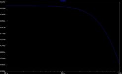
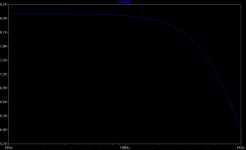
Some more simulations
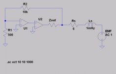
Here we have the block diagram of a classic SS amp under back EMF drive.
U1 is the input/VAS stage (gain=2K), U2 is the emitter follower stage (gain=0.9), Zout is the follower's equivalent output impedance, closed loop gain 21 dB, feedback 40 dB.
Rs and Ls are the speaker's resistence and inductance; EMF is the generator.
Attachments
....But what "input" does the differential sees? I have strong suspicion that the "input" (differential) is not seeing the input signal ONLY, the differential sees inputsignal+backEMF as it's "input".... [/B]
This is exactly what happens and it's OK. To put it in other words, let's look signals *backwards* i.e. going from output to input.
Assume we have a forward gain (main amplifier) with exponential transfer characteristic instead of linear.
Think now we have it connected with heavy negative feedback and apply whatever signal you want. A sinusoid is perfectly valid.
We know the output will be very close to a sinusoid too, only with a vanishigly small distortion, the higher the loop gain the lower the distortion.
Going now backwards, since the amplifier has an exponential transfer, its (differential) input cannot be a sinusoid, but rather a *predistorted* sinusoid (in fact a sinusoid to which an inverse exponential or logaritmic compression has been applied).
How did we achieve this? That is, generate an input signal that matches in reverse form the amplifier exponential transfer?
Simply substracting from the input signal a sample of the output. Since the output is slightly distorted still, when the undistorted input is substracte we are left with the desired waveform, that required to - after passing through the amplifier - reproduced a close copy of the desired input.
This lengthy description only tries to visualize what's going on. The important thing is the math predicts how feedback works, and the bench confirms it.
With respect to back EMF, since it was not present in the input, it is wholly reversed and added at the input to cancel it. Of course full cancellation is not possible, for in this case there should be no error signal to feed back, so a small amount will allways be there.
This efect of "damping" back injected voltage is equivalent to stating the amplifier has a low output impedance, that is, a voltage source very resilient to externally applied perturbations.
Rodolfo
Hi, Rodolfo,
Is it that simple to join [adding or substracting] with [exponential or 1/exponential] gain characteristic? Those 2 math action cannot be joined that easily (to get linear result), I think.
But this can explain why inverting and non-inverting sounds different (to some people).
In inverting mode, the input and feedback is put directly to 1 path, happens before entering any base, and the result of the [adding or substracting] is going to 1 base of transistor only. So the [adding or substracting] happens only with resistors, and happens before entering any base (which has not-linear characteristic). The other base (the left base) holds steady at 0 ground point without any excitation to it.
So in inverting mode, the right left base of differential is not working as 1/2 of differential, but it is working only as a "VOLTAGE REFERENCE" for the right differential half.
In non-inverting mode, left and right bases are both excited by signal. Left by input signal and right by feedback signal. The 0 point (where the excitation should be 0) is in the point of joint of both emitors (where the 2 emitors meet the CCS).
You can see, that for any signal in inverting mode to reach 0 point, it has to pass a B-E junction. The input signal (left) has to pass 1 B-E junction, and the feedback (right) also has to pass 1 B-E junction, while the relation of this B-E junction is not linear.
In non inverting mode, the summing signal only happens with resistors, and happened before entering any B-E junction.
To me it makes sense if some people can hear the difference of inverting and non-inverting topology. The key point is B-E junction. What E gives cannot be 100% copy of what B receives (even it is called emitor follower mode)
Simply substracting from the input signal a sample of the output.
Is it that simple to join [adding or substracting] with [exponential or 1/exponential] gain characteristic? Those 2 math action cannot be joined that easily (to get linear result), I think.
But this can explain why inverting and non-inverting sounds different (to some people).
In inverting mode, the input and feedback is put directly to 1 path, happens before entering any base, and the result of the [adding or substracting] is going to 1 base of transistor only. So the [adding or substracting] happens only with resistors, and happens before entering any base (which has not-linear characteristic). The other base (the left base) holds steady at 0 ground point without any excitation to it.
So in inverting mode, the right left base of differential is not working as 1/2 of differential, but it is working only as a "VOLTAGE REFERENCE" for the right differential half.
In non-inverting mode, left and right bases are both excited by signal. Left by input signal and right by feedback signal. The 0 point (where the excitation should be 0) is in the point of joint of both emitors (where the 2 emitors meet the CCS).
You can see, that for any signal in inverting mode to reach 0 point, it has to pass a B-E junction. The input signal (left) has to pass 1 B-E junction, and the feedback (right) also has to pass 1 B-E junction, while the relation of this B-E junction is not linear.
In non inverting mode, the summing signal only happens with resistors, and happened before entering any B-E junction.
To me it makes sense if some people can hear the difference of inverting and non-inverting topology. The key point is B-E junction. What E gives cannot be 100% copy of what B receives (even it is called emitor follower mode)
Lumunauw,
Whether it's non-inverting or inverting the comparison is base to base (or gate to gate). The only difference is a common mode signal equal to the input or feedback signal level for the non-inverting and zero (=GND) common mode signal for the inverting.
In listening to the two configurations (say if you could just switch between them), one will have CM distortion added depending on the CM quality of it's input stage plus a slightly increased gain (NI), while the other will have no common mode distortion added and slightly less gain (Inverted).
Cheers,
Greg
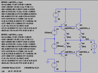
A while back in this thread, there was discussion about power amp output transistor models. I came up with a model for the MJL3281a that was a tweaked version of the OnSemi model, modified so its DC parameters were a much better fit to the data sheet characteristic curves than the standard one. I cloned this model to a PNP as well, making a symettric pair. I put these in the simulated circuit below, with a stepped DC current source as the load, going from -20 A to +20 A. This circuit has 0.22 Ohm emitter resistors, with the bias current adjusted to Self's optimum value for this configuration, 107 mA per device.
I plotted V vs I, which wasn't very interesting. But there's also the undocumented LTSpice d() plot function, which takes the derivative and plots it. This is more interesting, as it gives the output impedance at DC as a function of load current. In reality, this could be a multi-dimensional nonlinearity - that is, the output impedance could be a function of both output current and voltage, but I'll neglect that for now. Also, it would be more realistic to have a non-zero resistor from the junction of the two bias voltage sources to ground. A picture of the test simulation circuit is below.
I plotted V vs I, which wasn't very interesting. But there's also the undocumented LTSpice d() plot function, which takes the derivative and plots it. This is more interesting, as it gives the output impedance at DC as a function of load current. In reality, this could be a multi-dimensional nonlinearity - that is, the output impedance could be a function of both output current and voltage, but I'll neglect that for now. Also, it would be more realistic to have a non-zero resistor from the junction of the two bias voltage sources to ground. A picture of the test simulation circuit is below.
Attachments
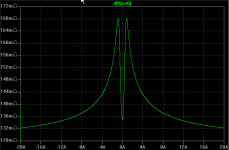
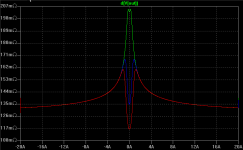
The output impedance vs current is shown in the graph below.
One interesting thing might be to try to duplicate this behavior as a nonlinear one-port using controlled sources that are polynomials. This might be done using MathCad or a similar tool to fit the I/V curve. Then, this nonlinear impedance could be put in series with an ideal, distortionless voltage source. Any computed distortion would then be due only to the impedance nonlinearity and its interaction with the load. The effects of feedback on this distortion could also be examined.
One interesting thing might be to try to duplicate this behavior as a nonlinear one-port using controlled sources that are polynomials. This might be done using MathCad or a similar tool to fit the I/V curve. Then, this nonlinear impedance could be put in series with an ideal, distortionless voltage source. Any computed distortion would then be due only to the impedance nonlinearity and its interaction with the load. The effects of feedback on this distortion could also be examined.
Attachments
 Seriously though, I could be talked into that if you're really interested in looking at it. There will be some asymmetry I'm sure, as well as some minor DC offsets.
 Not last time I looked.
- Status
- This old topic is closed. If you want to reopen this topic, contact a moderator using the "Report Post" button.
- Home
- Amplifiers
- Solid State
- The many faces of distortion