THE Simple RAIL TO RAIL SWINGER N-CHANNEL MASTER AMP
Hello to everyone,
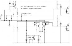
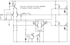
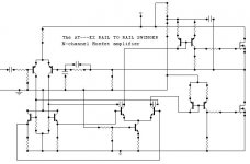
Presented here is a simple n-channel mosfet amp [block diagram]capable of delivering rail to rail swing without the need of extra complexities such as seperate driver supplies to keep the regular DIYer in a simple and safe state at the same time enjoying the pleasure of using N-channel mosfets.
Suggestion and comments , subjective or objective, constructive or destructive criticism are most welcome to further develop it into a design which will be a very simple and easy to build a excellent sounding amp.
So comment and enjoy the spirit of DIYING
Cheers,
Kanwar")
Hello to everyone,
Presented here is a simple n-channel mosfet amp [block diagram]capable of delivering rail to rail swing without the need of extra complexities such as seperate driver supplies to keep the regular DIYer in a simple and safe state at the same time enjoying the pleasure of using N-channel mosfets.
Suggestion and comments , subjective or objective, constructive or destructive criticism are most welcome to further develop it into a design which will be a very simple and easy to build a excellent sounding amp.
So comment and enjoy the spirit of DIYING
Cheers,
Kanwar
Attachments
To saturate it till its limit and squeeze max efficiency out of it.
just a simple design although , by the way what are your comments about the design. Since its a straight forward design with no complexites involved , therefore one has to comment it on it according to his own perspective view.
just a simple design although , by the way what are your comments about the design. Since its a straight forward design with no complexites involved , therefore one has to comment it on it according to his own perspective view.
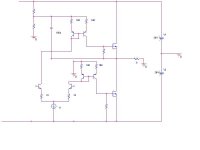
I see the reason for the bootstrapped divider for the top N-ch output FET as you need more than the +V rail to get it fully on. But on the bottom end the divider could just as well have been connected to ground, not the output, as you really have nothing to bootstrap. In fact, it would be even better if it was a single resistor from ground as the voltage swing is fairly small compared to the DC from ground to the gate of the bottom FET, hence it would better approximate a current source, like the upper bootstrapped version does.
ilimzn said:I see the reason for the bootstrapped divider for the top N-ch output FET as you need more than the +V rail to get it fully on. But on the bottom end the divider could just as well have been connected to ground, not the output, as you really have nothing to bootstrap. In fact, it would be even better if it was a single resistor from ground as the voltage swing is fairly small compared to the DC from ground to the gate of the bottom FET, hence it would better approximate a current source, like the upper bootstrapped version does.
In my simulation,when I eliminate the bootstrap on lower mosfet, and followed your comment, the lower rail loss rises from 0.65 to 2 volts. which is a decrease in efficiency.
The way I see it is that the bottom end divider maintains the VAS current irrespective of output voltage level, similar to the way that the bootstrap does it for the other half.
The only issue I can see is that the two halves of the VAS will see different collector voltages, so they will run at different temperatures. I don't know how inportant this will be in practice.
The only issue I can see is that the two halves of the VAS will see different collector voltages, so they will run at different temperatures. I don't know how inportant this will be in practice.
johnnyx said:The way I see it is that the bottom end divider maintains the VAS current irrespective of output voltage level, similar to the way that the bootstrap does it for the other half.
The only issue I can see is that the two halves of the VAS will see different collector voltages, so they will run at different temperatures. I don't know how inportant this will be in practice.
There would a difference in temperatures between VAS transistors, but they must be mounted on the heatsink which will provide them thermal safety and there would be no practical problem in reality.
That really does not make any sense unless the schematic you posted is not the same as the one your simulator is using.
You have a divider from output to gate drive of the bottom FET, the midpoint of the divider is connected to -V rail through a capacitor. Assuming perfectly stiff rails (fair assumption for a simulator), and a decent size capacitor, the top of the divider is at 0V DC (that should be the DC component of the output!), the bottom of the divider is a Vgsbias. The current through the bottom resistor is (voltage on capacitor - Vgsbias)/(bottom resistor). You should be able to replace the capacitor with a voltage source equal to the DC operating point voltage on the capacitor with no change at all in performance. So, if you can do that, you could just as well connect one resistor to ground, it'svalue equal to the total resistance of the divider, so you get the same current. Or has someone gone and changed Ohm's law while I was asleep?
Also, your input cap to ground needs to be put after the input resistor divider or it will not filter anything from a voltage source at the input (even though there are no true voltage sources, it will confuse the heck of the ones trying to be, and may even resonate with the cable inductance).
The bias generator needs carefull attention. As you have it now, it compensates itself very well (Vbe of CCS with Vbe of the diode connected transistor) but not the FETs, or rather, the current tracks the _difference_ between the CCS temperature and the FET temperature if the diode connected transistor is on the heatsink with them, instead of FET absolute temperature. Correct tracking also relies on the resistor dividers in the FET drivers vs actual current chosen as well as the actual voltage reference of the CCS chosen (the zener and the trimmer, the tracking law changes with the bias current chosen). Seems a bit touchy to me...
ilimzn said:That really does not make any sense unless the schematic you posted is not the same as the one your simulator is using.
You have a divider from output to gate drive of the bottom FET, the midpoint of the divider is connected to -V rail through a capacitor. Assuming perfectly stiff rails (fair assumption for a simulator), and a decent size capacitor, the top of the divider is at 0V DC (that should be the DC component of the output!), the bottom of the divider is a Vgsbias. The current through the bottom resistor is (voltage on capacitor - Vgsbias)/(bottom resistor). You should be able to replace the capacitor with a voltage source equal to the DC operating point voltage on the capacitor with no change at all in performance. So, if you can do that, you could just as well connect one resistor to ground, it'svalue equal to the total resistance of the divider, so you get the same current. Or has someone gone and changed Ohm's law while I was asleep?
Also, your input cap to ground needs to be put after the input resistor divider or it will not filter anything from a voltage source at the input (even though there are no true voltage sources, it will confuse the heck of the ones trying to be, and may even resonate with the cable inductance).
The bias generator needs carefull attention. As you have it now, it compensates itself very well (Vbe of CCS with Vbe of the diode connected transistor) but not the FETs, or rather, the current tracks the _difference_ between the CCS temperature and the FET temperature if the diode connected transistor is on the heatsink with them, instead of FET absolute temperature. Correct tracking also relies on the resistor dividers in the FET drivers vs actual current chosen as well as the actual voltage reference of the CCS chosen (the zener and the trimmer, the tracking law changes with the bias current chosen). Seems a bit touchy to me...
Hi ilimzn,
The Cap is not at the midpoint of resistor divider and the ratio of voltage divider is set, such that the caps voltage will remain at around 15Volts with respect to ground under no signal conditions in order to ensure perfect drive condition with no overdriven on gate.
I doesnot like your opinion of replacing cap with voltage source because it hampers the symmetry of output gate drive characteristics. No one has changed Ohms law , but maybe your perspective have changed a little bit due to sleeplessness.
regarding the input cap, its a drawing error which will be corrected.Thanks for the comment.
Regarding bias generator, i sees your point too. Its connected in a wrong way.
Then whats your suggestion for it.
Attachments
hi Kanwar
another things:
1. Your PSRR would be ugly... it may even not work correctly with a bit variable rails
2. Is it open loop current source or voltage source?
Most N-ch amps are current sources, 'cause you change Vgs of both mosfets.
In your amp upper mosfet seems to play as a follower (voltage source) and lower as current source. It cannot work (in class AB/B at least), 'couse I and V may be not in phase, I mean positive V, negative I or otherwise, which can never happen in your amp.
Just thoughts...it's quite late though, I may be wrong..
regards
darkfenriz said:hi Kanwar
another things:
1. Your PSRR would be ugly... it may even not work correctly with a bit variable rails
2. Is it open loop current source or voltage source?
Most N-ch amps are current sources, 'cause you change Vgs of both mosfets.
In your amp upper mosfet seems to play as a follower (voltage source) and lower as current source. It cannot work (in class AB/B at least), 'couse I and V may be not in phase, I mean positive V, negative I or otherwise, which can never happen in your amp.
Just thoughts...it's quite late though, I may be wrong..
regards
Hello DarkfenriZ,
How would you say that PSRR willnot be that good, I simply donot see any reasons for this , If you really see , then intimate me with reasonableness.
The upper mosfet works as Source Follower and lower mosfet works as Common Source amplifier, whose gates are controlled by string master differentials which in turn act as current sources as well.
Kindly get some good sleep and think again in the morning and attack with some more robustness............
hallo Kanwar
now I am awaken but still before morning cofee
so let's think it over again:
1. As the second stage you use a long tailed pair and the tail current is fixed, right?
OK. and the voltage driving output mosfets is produced by drop on collector resistrors of LTP. For simplicity let's analyse what's going on when idle, no input, Vout=0.
Voltage drop on collector resistors is :
Rc*tail current/2
Voltage on the gate of upper mosfet=+Vrail-Rc*tail current/2
Voltage on the gate of lower mosfet=-(-Vrail)-Rc*tail current/2
So voltages on gates are depending on rails voltages making the amp either balancing between class A and C or have low PSRR.
2.
Apart from reactive load issues, source follower needs voltage swing on gate equal (of even a bit bigger) to output V swing.
Common source amplifier needs just little voltage swing to make the channel on and off. And it is hard to predict the proportion...
regards
now I am awaken but still before morning cofee
so let's think it over again:
1. As the second stage you use a long tailed pair and the tail current is fixed, right?
OK. and the voltage driving output mosfets is produced by drop on collector resistrors of LTP. For simplicity let's analyse what's going on when idle, no input, Vout=0.
Voltage drop on collector resistors is :
Rc*tail current/2
Voltage on the gate of upper mosfet=+Vrail-Rc*tail current/2
Voltage on the gate of lower mosfet=-(-Vrail)-Rc*tail current/2
So voltages on gates are depending on rails voltages making the amp either balancing between class A and C or have low PSRR.
2.
The upper mosfet works as Source Follower and lower mosfet works as Common Source amplifier,
Apart from reactive load issues, source follower needs voltage swing on gate equal (of even a bit bigger) to output V swing.
Common source amplifier needs just little voltage swing to make the channel on and off. And it is hard to predict the proportion...
regards
darkfenriz said:hallo Kanwar
now I am awaken but still before morning cofee
so let's think it over again:
1. As the second stage you use a long tailed pair and the tail current is fixed, right?
OK. and the voltage driving output mosfets is produced by drop on collector resistrors of LTP. For simplicity let's analyse what's going on when idle, no input, Vout=0.
Voltage drop on collector resistors is :
Rc*tail current/2
Voltage on the gate of upper mosfet=+Vrail-Rc*tail current/2
Voltage on the gate of lower mosfet=-(-Vrail)-Rc*tail current/2
So voltages on gates are depending on rails voltages making the amp either balancing between class A and C or have low PSRR.
regards
Hi DarkfenriZ,
I see your point regarding biasing string, to overcome this one could implement constant current sources in place of upper Rc of both mosfets, to ensure good PSRR. Thanks for making the circuit better.
regards,
Kanwar
- Status
- This old topic is closed. If you want to reopen this topic, contact a moderator using the "Report Post" button.
- Home
- Amplifiers
- Solid State
- NVMOS amplifier