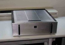
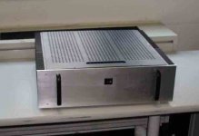

6 Channel amp
Ok...I will try and answer as many questions as possible.
The output devices are one pair ON semiconductor MJ15003/MJ15004 as perscribed by professor Leach (4 devices per channel). There is a "super" version of the same amplifier that uses 2 pair (8 total) with double the output specs. I have not communicated with Mr. Leach in some time, however I believe he still sells pcb boards for his amplifier. For more information on the Leach amp and contact information visit http://users.ece.gatech.edu/~mleach/lowtim .
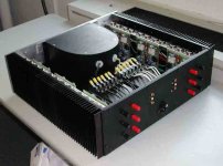
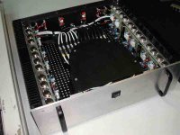
One of the reasons I made my own pcb boards was I wanted double sided connectors for the power and transistors. This allowed me to mount all the power and transistors from the BACK of the boards, which hides all the wiring and makes things look a bit neater.
The capaitors are not really "enclosed", more "covered". I used the 10000 uf 63V caps from APEXJR...unbelievably cheap at $1.50 each. These are snap in caps. So I made PCB boards to mount the caps in, and then covered the copper with 1/4 inch plastic. The cover was both for aesthetic reasons and to keep me from accidently touching the otherwise exposed capacitor bank") Plus I could then mount the fuses on the covers...which made the fuses accessable.
Plus I could then mount the fuses on the covers...which made the fuses accessable.
The heatsink is actually several pieces, which I had to cut/grind to make one big heatsink. For normal listening heat disipation is no problem. At high levels into 4 ohms it starts getting pretty warm...so maybe I will have to add some air flow to facilitate cooling.
Grounding....here is where I took a chance. Dr. Leach recommends a single grounding point. However this means having wires running all over your chassis, which I wanted to avoid. So befor I mounted the boards/trasistors, I took a large ring terminal and crimped/soldered 9 ground wires into it (2 per board X 3 boards + 1 per board output) I then removed one of the 1/4 inch bolts used to connect the heatsinks to the chassis, and used this bolt to clamp the ring terminal. This allowed me to cut all the ground wires to length, and keep all the wires behind the pcb boards, making things a bit neater. The amp is completely silent, I have not experienced any ground loops or other problems, so maybe I got away with this grounding solution.
Sound. I personally think this is a fine design. I spent quite a bit of time buying extra MPS8099/MPS8599 transistors and measuring HFE of each to get 4 matched transistors for each board. This paid off. My other leach amp has a tiny bit of DC offset (I did not match transistors on the first one). The 6 channel amp is dead silent. Even with your ear right up against the speaker there is no noise. So while the extra effort paid off now I have to get more transistors to fix the other amp ;P
Things I would do differently. Well, you can never have too much heatsink. I could have run the power wires along the front, which would isolate them physically, and I could have built a conduit so the wires would be covered...oh well maybe on the next project...
Ok...I will try and answer as many questions as possible.
The output devices are one pair ON semiconductor MJ15003/MJ15004 as perscribed by professor Leach (4 devices per channel). There is a "super" version of the same amplifier that uses 2 pair (8 total) with double the output specs. I have not communicated with Mr. Leach in some time, however I believe he still sells pcb boards for his amplifier. For more information on the Leach amp and contact information visit http://users.ece.gatech.edu/~mleach/lowtim .
One of the reasons I made my own pcb boards was I wanted double sided connectors for the power and transistors. This allowed me to mount all the power and transistors from the BACK of the boards, which hides all the wiring and makes things look a bit neater.
The capaitors are not really "enclosed", more "covered". I used the 10000 uf 63V caps from APEXJR...unbelievably cheap at $1.50 each. These are snap in caps. So I made PCB boards to mount the caps in, and then covered the copper with 1/4 inch plastic. The cover was both for aesthetic reasons and to keep me from accidently touching the otherwise exposed capacitor bank
Plus I could then mount the fuses on the covers...which made the fuses accessable.The heatsink is actually several pieces, which I had to cut/grind to make one big heatsink. For normal listening heat disipation is no problem. At high levels into 4 ohms it starts getting pretty warm...so maybe I will have to add some air flow to facilitate cooling.
Grounding....here is where I took a chance
. Dr. Leach recommends a single grounding point. However this means having wires running all over your chassis, which I wanted to avoid. So befor I mounted the boards/trasistors, I took a large ring terminal and crimped/soldered 9 ground wires into it (2 per board X 3 boards + 1 per board output) I then removed one of the 1/4 inch bolts used to connect the heatsinks to the chassis, and used this bolt to clamp the ring terminal. This allowed me to cut all the ground wires to length, and keep all the wires behind the pcb boards, making things a bit neater. The amp is completely silent, I have not experienced any ground loops or other problems, so maybe I got away with this grounding solution.Sound. I personally think this is a fine design. I spent quite a bit of time buying extra MPS8099/MPS8599 transistors and measuring HFE of each to get 4 matched transistors for each board. This paid off. My other leach amp has a tiny bit of DC offset (I did not match transistors on the first one). The 6 channel amp is dead silent. Even with your ear right up against the speaker there is no noise. So while the extra effort paid off now I have to get more transistors to fix the other amp ;P
Things I would do differently. Well, you can never have too much heatsink. I could have run the power wires along the front, which would isolate them physically, and I could have built a conduit so the wires would be covered...oh well maybe on the next project...
Hi,
you have adopted Leach grounding scheme i.e. resistor between signal ground and power ground then power ground direct to chassis ground.
Does you PCboard star connect each clean ground and separately star connect each power ground?
Have you run a ground wire from each insulated input connector to the respective driver board?
I have not tried this scheme but it seems to have worked for you & with 6 channels.
You mention 3 channels into your master ground. Do you have a separate master ground for the other 3 channels?
Info on matching, what tolerance?
Thanks for taking the time to compile that reply
Grounding
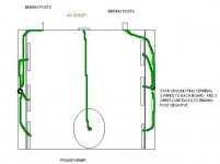
Sorry I should have elaborated. THe right/left sides are symetrical, each has a ring terminal with 9 wires on it bolted to the frame, which provides star grounding for the three boards and three negative binding posts on that side of the amplifier. The AC ground is connected to the 3/8 inch bolt which holds in the torridal transformer. So there are 3 grounding points rather than the single star topology recommended by Mr. Leach. I have attached (a somewhat crude) picture that may help in clarifying the grounding.
Sorry I should have elaborated. THe right/left sides are symetrical, each has a ring terminal with 9 wires on it bolted to the frame, which provides star grounding for the three boards and three negative binding posts on that side of the amplifier. The AC ground is connected to the 3/8 inch bolt which holds in the torridal transformer. So there are 3 grounding points rather than the single star topology recommended by Mr. Leach. I have attached (a somewhat crude) picture that may help in clarifying the grounding.
Attachments
Transistor matching
Allmost forgot to answer the transistor matching. Basically the matching was exact. I tried measuring the transistors several different ways, and got inconsistant results. Finally I got my hands on a multimeter that measures transistor HFE. By this time I had 100+ EACH of MPS8099/MPS8599/MPSA06/MPSA56. So I measured all the transistors I had, made a big list and came up with 6 sets of 4. The good part is multimeters that measure HFE are cheap...and so are the transistors.
Allmost forgot to answer the transistor matching. Basically the matching was exact. I tried measuring the transistors several different ways, and got inconsistant results. Finally I got my hands on a multimeter that measures transistor HFE. By this time I had 100+ EACH of MPS8099/MPS8599/MPSA06/MPSA56. So I measured all the transistors I had, made a big list and came up with 6 sets of 4. The good part is multimeters that measure HFE are cheap...and so are the transistors.
PCB layout
I hesitate to post a modified schematic without Mr.Leachs approval. However the changes I made are simple. If you look at the layout http://users.ece.gatech.edu/~mleach/lowtim/graphics/layouts.pdf
And at the parts layout, you will see that the output transistors Q18,Q19,Q20,Q21 have 3 leads each which connect to the board. All I did was add a solder point on the other side of the board (the boards are normally single sided). I used techniks "press and peel blue" (fantastic stuff) to make the layout for the single sided boards. I drilled the transistor holes so I could identify the exact location and added the solder points on the other side of the board. I also did this with the -/+ power connections and grounding points.
- Status
- This old topic is closed. If you want to reopen this topic, contact a moderator using the "Report Post" button.
- Home
- Amplifiers
- Solid State
- 6 channel amp finished