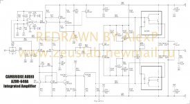
The NE5534 is a DC servo but the output isn't drawn correctly. The output isn't connected to any load.
I have a similar servo in my QRV-03 amp.
I have a similar servo in my QRV-03 amp.

Gasho said:Here is shematic.
A kind of an unconnected overload detector (diff.amp).
peranders said:The NE5534 is a DC servo but the output isn't drawn correctly.
Where in your opinion should the output be connected?
Take a look at RC values.
Regards,
Milan
why I must to put a trimpot i series with R2
Because you can make life difficult or easy for an opamp.
The schematic appears to have many errors, the unconnected output of the NE5534 is only one - the connection of the 'clip detect' and output transistors does not make much sense, for instance.
The 5534 seems to be a clip detector, but the output is drawn unconnected. The reason DC offset voltage changes when you change the resistor is that the combined bias current of the NE5534 (which is quite high, BTW) and the amp itself develops different voltages at the differential pair inputs, and you get this difference as an output offset. It remains a mystery why anyone would use a NE5534 in this application, but I guess if every chip in the amp is a NE5534, economy of scale applies - it may just have been the least expensive to use.
As for your proposal to reduce NFB - this also increases closed loop gain, from roughly 34 to 51, which also reduces bandwidth in proportion, and increases distortion. Why would you want to do this?
If you want to reduce NFB (which is not something to be done unless you know exactly what you are doing and why), you need to reduce open loop gain and keep closed loop gain the same. There are a number of ways you could do this on this amp, and the best ones have nothing to do with R65. If you are competent enough to arrive at the decision that NFB should be reduced, you should easily be competent enough to know what these methods are, and which one is the best to use.
ilimzn said:The schematic appears to have many errors
....
I add strange cascoded VAS
I also agree it is cliping detector - look at C value
Well, it is difficult to judge how sound it is considering the errors in the schematic. But there are several things (discounting obvious errors) that I find odd:
1) The composite current source for the LTP and the VAS - OK, I know there's a pretty stable 2 x Vbe there in the current source but using that as a reference for another current source is really corner cutting at it's worst.
2) Darlington in the VAS? Probably a drawing error... BTW don't see anything wrong with a cascoded VAS, this is used quite often especially for VAS operating with higher currents, because it gives you freedom to use a high gain and high FT transistor which would normally not be able to take the required dissipation for the current gain, and have most of the heat developed on the cascode transistor.
3) OK, not the usual stuff using a single ended follower oaded with a current source as a driver stage, at least it operates in class A. But what is that 18k resistor to the -V rail? An odd way to stability?
- Status
- This old topic is closed. If you want to reopen this topic, contact a moderator using the "Report Post" button.
- Home
- Amplifiers
- Solid State
- What is the purpose of NE5534 in this amp