Class AB amplifiers are so popular because they can produce substantial power output far cheaper and without the size weight and cost penalties of class A. They also consume substantially less power than equivalent Class A and as such are substantially more environmentally friendly.
But designing one is not as simple as just turning down the output stage bias of an equivalent Class A design. Many of these are the picture of simplicity and it's relatively easy to get a good sound and that's why they've become a fallback position for some manufacturers unknowledgeable of how to deal with the distortions generated by the output stage switching and end up in desperation turning the bias up maybe half way, fitting huge heatsinks, continuous duty regulated supplies and promote largesse as the way to audio nirvana.
I worked for one such company and it was a real eye opener. In my short time there I designed and prototyped a lightweight low bias Class AB power amplifier from parts lying around there and it blew those high bias behemoths away. How did I do it? Simple.
I had this in the FRONT of my mind when designing the topology, the PCB layout and the chassis geography.
What's the schematic looks like? Is it something different than ordinary low biased classAB looks like? Or it doesn't have to do with schematic, just pcb and chassis geography?How did I do it? Simple.
Lumanauw,
It's not a specific topology. It's more about approach. It's about awareness that such voltages and consequent currents are lurking everywhere around the output stage and drivers radiating fields and modulating power supplies. They are there waiting at the periphery of your design looking for a weak point to intrude.
And most people give them numerous opportunities starting with the simple miller comp Vas. Straight down the PSRR route or in through that too close input stage or coupled through that sloppy wiring loom.
It pops up on the spectrum analyser as harmonic emphasis as you juggle the wiring loom for best results.

Don't you get easily rid of this by using a full H-Bridge ?
At least none of these half-waves are disturbing the psu this way,
as the load is always symetrical.
Of course you still have these pulses in the wires to the outputbjts...
Does it help placing a big cap from collector of upper device
to collector of lower device ? (For EF) Very close of course...
Mike
.MikeB said:Don't you get easily rid of this by using a full H-Bridge ? At least none of these half-waves are disturbing the psu this way, as the load is always symetrical.
Of course you still have these pulses in the wires to the outputbjts...
Mike, you still get pulses in the rails, just full-wave rectified load current, not half wave. You only get unrectified load current in class A.
balanced approach still has advantages, as you only have one set of twi wires to contend with, and most of the magnetic induction problems get solved by using a twisted pair for them.
Another possibility for regular split supply class (A)B is to braid the wires for +V, -V and ground, because sum of +V and -V current equals -(load current). Unfortunately, braiding does not produce as low loop area as twisting. In theory, twisting all three together will work best but unlike a braid, or two twisted wires, 3 twisted wires do not tend to keep together as well.
'guru;
I think I understand what your getting at. But let me ask some direct questions if you would.
I've been educated to believe that pcb layout should have the input stage as compact as possible.
The vas should also be compact, but separated from the i/s by a reasonable distance.
The drivers and outputs should be as spread out as possible, within reason. Also, o/p should be moved away from the first two stages.
That power supplies should be far from the pcb. Some have even told me that magnetic shielding of the p/s is better. I've seen some techs add a nickle braided wire into the supply loom and twist it with the pair. Grounding it to the case and a ground point on the board for shielding. Note; I see this trick on ford diesel trucks to shield the 115vdc injector driver circuits. Shielding makes since to me.
I hope I haven't buchered your points here. Let me know what you think.
Roger
Hi Roger.
Sorry I didn't respond earlier I've been trying to get a PC soundcard based test set working right so I can pull some live illustrations to >16 bit.
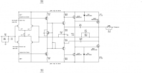
I always design a power amp PCB with the unreg supply lines (=V,-V,gnd) coming into the board perpendicular and twisted, sometimes in a braided sheath. They then distribute to a heavily bypassed output stage through very short tracks.
The feed to the Vas and earlier stages is thin and ground planed with only local currents. The design of these stages suppresses intrusion by one or more techniques -
regulators , cascoding , differential loading , or op-amp.
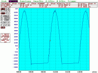
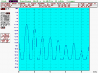
The rubbish on these unregulated lines exposed to the early stages is only voltage (no half currents near) contains all the harmonics shown, in response to a pure tone plus very low freq supply power demand modulation and 100-120Hz ripple.
All these depend on supply impedance. which can be halved by doubling supply caps and transformer and supply tracks i.e. 6 dB improvement by massive doubling supply weight OR
30-40dB and upwards improvement by improving rejection by the methods earlier.
As much of it is low freq, an op amp gain characteristic is good and indeed a good chip (say OPA627)driven amp with even zener regulators works a treat.
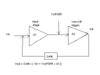
For example , assuming a convential amplifier design the weak spot is the output divider from the input stage/input to the Vas, especially as the miller cap kicks in and kills the PSRR at higher frequencies. One each side for a symmetrical design.
more...
Sorry I didn't respond earlier I've been trying to get a PC soundcard based test set working right so I can pull some live illustrations to >16 bit.
I always design a power amp PCB with the unreg supply lines (=V,-V,gnd) coming into the board perpendicular and twisted, sometimes in a braided sheath. They then distribute to a heavily bypassed output stage through very short tracks.
The feed to the Vas and earlier stages is thin and ground planed with only local currents. The design of these stages suppresses intrusion by one or more techniques -
regulators , cascoding , differential loading , or op-amp.
The rubbish on these unregulated lines exposed to the early stages is only voltage (no half currents near) contains all the harmonics shown, in response to a pure tone plus very low freq supply power demand modulation and 100-120Hz ripple.
All these depend on supply impedance. which can be halved by doubling supply caps and transformer and supply tracks i.e. 6 dB improvement by massive doubling supply weight OR
30-40dB and upwards improvement by improving rejection by the methods earlier.
As much of it is low freq, an op amp gain characteristic is good and indeed a good chip (say OPA627)driven amp with even zener regulators works a treat.
For example , assuming a convential amplifier design the weak spot is the output divider from the input stage/input to the Vas, especially as the miller cap kicks in and kills the PSRR at higher frequencies. One each side for a symmetrical design.
more...
Attachments
Hi guru
Hi guru,
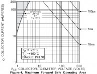
Would you please tell me something?")
How much power handling capacity does this device may give when operated from +-80V dc with ambient temperature of environment 50. C. and forced cooling is used.
mounted directly on heatsink with dual side efficient cooling
This is the SOA curve of 600V, 100A IGBT.
regards,
Kanwar
Hi guru,
Would you please tell me something?
How much power handling capacity does this device may give when operated from +-80V dc with ambient temperature of environment 50. C. and forced cooling is used.
mounted directly on heatsink with dual side efficient cooling
This is the SOA curve of 600V, 100A IGBT.
regards,
Kanwar
Attachments
Hi Kanwar,
Big is beautiful, right?
Lets see 600V /100A IGBT - probably APT?
APT100GF60LR 390W plastic flat pack good for 20KHz if you can drive it. Cin is 4n4 , Qg 126nC, rise/fall 400nS from 10ohms .
As a developmental starting point I'd start with an expectation of 5A at 80V (pkg rating) and depending on your output stage topology allow 10-15A peak, given a Vge of 5.5V thats a lot of dissipation unless you use a design that reduces output stage losses.
You seem to favour extreme heatsinking behemoth devices rather than spreading between many agile alternatives. Why is that?
Hi guru
Hi guru ,
your guess is right about the identity of device which is from APT.
As per your expectation is concerned , We have tested this IGBT in our project amplifier .Since this IGBT is fabricated using APT's advanced high power density wafer processing , which inturn enables very high power density in to this package.
We have developed a unique pushpull current drive driver stage of each IGBT in upper and lower rail with seperate power supplies , which drives these monsters to full saturation that is near rail swing.
The output stage features near rail to rail swing with a very little voltage drop of 3 volts at 2 ohms operation which cuts out the phenomena of rail loss which is especially found in some mosfet amps. We have been able to extract as much as 1300Wrms from just single pair of devices mounted directly on heatsinks with room temp at about 45deg celcius and heatsink temp around 68deg.
Some measurements:
device biasing at 200mA with Vge at 5.8Volts
VCC=+-80VDC.
Peak current measured below the limit of device destruction was around 55amperes peak.
Continuous current with 1kHz sine wave input =25 amperes rms.
Stable into reactive loads .
We prefer lots of heatsinking because it gives a high thermal mass which inturns serves as an advantage in conditions relating to thermal stress or thermal overload during continuous long duration operation.
We prefer mammoth devices because they consume very less space as their is also no need for parallelling the devices which inturns consumes less fabrication time and speeds up the production. Secondly there is no need of matching the devices.
Besides this lots of headaches involved in paralleling are left out.
some guys might just dont believe what i have said , but that's everyones own...........?
regards,
Kanwar
amplifierguru said:Hi Kanwar,
Big is beautiful, right?
Lets see 600V /100A IGBT - probably APT?
APT100GF60LR 390W plastic flat pack good for 20KHz if you can drive it. Cin is 4n4 , Qg 126nC, rise/fall 400nS from 10ohms .
As a developmental starting point I'd start with an expectation of 5A at 80V (pkg rating) and depending on your output stage topology allow 10-15A peak, given a Vge of 5.5V thats a lot of dissipation unless you use a design that reduces output stage losses.
You seem to favour extreme heatsinking behemoth devices rather than spreading between many agile alternatives. Why is that?
Hi guru ,
your guess is right about the identity of device which is from APT.
As per your expectation is concerned , We have tested this IGBT in our project amplifier .Since this IGBT is fabricated using APT's advanced high power density wafer processing , which inturn enables very high power density in to this package.
We have developed a unique pushpull current drive driver stage of each IGBT in upper and lower rail with seperate power supplies , which drives these monsters to full saturation that is near rail swing.
The output stage features near rail to rail swing with a very little voltage drop of 3 volts at 2 ohms operation which cuts out the phenomena of rail loss which is especially found in some mosfet amps. We have been able to extract as much as 1300Wrms from just single pair of devices mounted directly on heatsinks with room temp at about 45deg celcius and heatsink temp around 68deg.
Some measurements:
device biasing at 200mA with Vge at 5.8Volts
VCC=+-80VDC.
Peak current measured below the limit of device destruction was around 55amperes peak.
Continuous current with 1kHz sine wave input =25 amperes rms.
Stable into reactive loads .
We prefer lots of heatsinking because it gives a high thermal mass which inturns serves as an advantage in conditions relating to thermal stress or thermal overload during continuous long duration operation.
We prefer mammoth devices because they consume very less space as their is also no need for parallelling the devices which inturns consumes less fabrication time and speeds up the production. Secondly there is no need of matching the devices.
Besides this lots of headaches involved in paralleling are left out.
some guys might just dont believe what i have said , but that's everyones own...........?
regards,
Kanwar
Really massive power transistors are uncommon and
generally unavailable at reasonable prices, so they
seldom figure into consumer equipment designs. Big
bipolar (and doubtless MOSFET) packages consisting
of either custom silicon or paralleled dies have been
out for decades; IGBTs are more recent and haven't
been particularly popular for whatever reason. I've
heard that distortion is higher due to higher turnon
voltages, and they're not as linear overall, making them more difficult to design with.
But the relative simplicity of physical amplifier design
certainly compensates.
Looks like you may be on the cutting edge of technology,
and in a position to be a leader, too. How much
do these high-power IGBTs cost and where can I get
samples?
--Damon
generally unavailable at reasonable prices, so they
seldom figure into consumer equipment designs. Big
bipolar (and doubtless MOSFET) packages consisting
of either custom silicon or paralleled dies have been
out for decades; IGBTs are more recent and haven't
been particularly popular for whatever reason. I've
heard that distortion is higher due to higher turnon
voltages, and they're not as linear overall, making them more difficult to design with.
But the relative simplicity of physical amplifier design
certainly compensates.
Looks like you may be on the cutting edge of technology,
and in a position to be a leader, too.
How much do these high-power IGBTs cost and where can I get
samples?
--Damon
- Status
- This old topic is closed. If you want to reopen this topic, contact a moderator using the "Report Post" button.
- Home
- Amplifiers
- Solid State
- What every Class AB builder needs to be constantly aware of