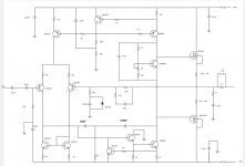
looks like a Self Blameless with VAS protection and a MOSFET output stage.
1000pF for miller compensation seems a bit large to me. Also you have an RC on the VAS base for more compensation - is this really neccesary ? If it's that unstable the sound won't be good.
Personally I would use driver transistors on the MOSFETs but that's just me. The 649/669's should work well for that.
coupled bias reference for the ltp and vas is not good, self fought asymmetric slew rate caused by this false economy in his early blameless designs - completely separate ccs circuits are too cheap to bother fixing up any interactions in your circuit
higher mirror degeneration R values would reduce the noise contribution of this stage - they should at least equal the diff pair emitter degeneration R values
2 pole compensation is interesting but the 1000 pF, 1 K loads the vas, eliminating some of the potential extra audio frequency loop gain, putting the network around a buffered vas might work, or you can rework the T network values; ~= C reduces output loading on the unbuffered vas
power mosfets are not particularly high input impedance at high frequencies, buffering the vas will reduce distortion appreciably - although the supply V suggests this is just a line amp?, if the fets are small enough your T network could be the biggest vas load
gate series R may be useful to prevent parasitic RF oscillations in the mosfets
the output fet source series R seem pointlessly small for mosfet outputs
1000pF for miller compensation seems a bit large to me. Also you have an RC on the VAS base for more compensation - is this really neccesary ? If it's that unstable the sound won't be good.
That just two pole compensation. Reduces THD at higher frequencies. Yes, it can be unstable but that usually only happens if you make the cap too small. 1000p is probably large enough to avoid that and once everything is working well it may be worthwhile reducing it in steps until signs of instability show up and then back up a step or two.
Continuing, 1000p is appropriate as long as the other is 200p. Typically they have a ratio of 1:5 or 1:10 or somewhere in between. The 1k resistor is also worth thinking about. Usually, 1k to 10k is workable range. Increasing it to 2-5k may add some stability is the caps are decreased.
All this may sound like I'm just quoting Self, which is true, but I've built a few of these and experimented with the values and confirmed for myself trhat it works out.
All this may sound like I'm just quoting Self, which is true, but I've built a few of these and experimented with the values and confirmed for myself trhat it works out.
The schematic is in need of dots where the connections are -- especially around the LTP current source, which looks a little wrong to me but I'm having to guess without any dots, and the transistors given IDs e.g. TR1. That way we can tell you about which bit of the circuit we mean ")
As others have mentioned the MOSFETs look wrongly connected/drawn.
As others have mentioned the MOSFETs look wrongly connected/drawn.
...And the 2SJ162 body diode connection is drawn wrong suggesting a MOSFET with reversed D and S terminals...
More than that. I think you wany the 2sk1058 on the top (+rail) and the 2sj162 on the bottom (-rail). The source side should face each other while the drains connect to the rails. It's very easy to loose track of which way around these things go --at least it is for me.
Reverse the diode, also the + connection of the 220 µF elco must be connected to gnd, this is because you used pnp transistors in the ltp.
Disagree. It's OK they way he has it. As a matter of fact, as I write this I'm listeneing to a very nice amp build with an LTP constructed exactly they way Si99 shows it. Nothing theoretical about it -- the thing works and works well.
Bobo1on1, you may want to take a second look. Perhaps you are thinking of an LTP that has been constructed withe current mirrors at the top (+) and CCS at the bottom (-). That works fine but the 2n5551's and 2n5401's swap places. You would also need to swap the VAS top for bottom as well if you did that.
While I'm looking at this, it also ocurrs to me that since the output section is just a pair of L-mosfets, which I assume need to be rearranged into a "source follower configuration that the Vbe-multiplier can be replaced with simply a 1k or 500 ohm trippot.
Si992, I don't know the inspiration for this amp, but if you can find a copy of Randy Slones amplifier book at the library you might want to see how he does the L-mos output sections. (Not the hybrid complementary feedback types through).
Si992, I don't know the inspiration for this amp, but if you can find a copy of Randy Slones amplifier book at the library you might want to see how he does the L-mos output sections. (Not the hybrid complementary feedback types through).
sam9 said:
Disagree. It's OK they way he has it. As a matter of fact, as I write this I'm listeneing to a very nice amp build with an LTP constructed exactly they way Si99 shows it. Nothing theoretical about it -- the thing works and works well.
Bobo1on1, you may want to take a second look. Perhaps you are thinking of an LTP that has been constructed withe current mirrors at the top (+) and CCS at the bottom (-). That works fine but the 2n5551's and 2n5401's swap places. You would also need to swap the VAS top for bottom as well if you did that.
I'm sure it works fine, it probably works even better when not using the elco and diode at all.
However the elco is there to minimise DC offset and when using PNP transistors in the ltp the DC offset is negative to ground, that is why the elco should have its + connection on gnd.
Before we go off and advise folks to eliminate the NFB cap, it might be a nice gesture to suggest they read the aricle "Amplifier Clipping Behavior" at sound.au.com. Though there may well be benefits, not everyone is going to think increasing the risk og damaging their speakers is worth it.
the 220 uF dc blocking cap in the feedback network really should be nonpolar and high enough V rating to render the diode moot, both properties are required for least distortion when using Al electrolytics in the signal path
the diode just clamps the V across a polar electrolytic to prevent its exploding (not likely with the series R) with a stuck-to-rail or input fault - sometimes anti-parallel diodes are used to allow a very low V rated cap of small physical size - dc offsets should never exceed a few mV in a properly working amp and the diode(s) should never conduct
the diode just clamps the V across a polar electrolytic to prevent its exploding (not likely with the series R) with a stuck-to-rail or input fault - sometimes anti-parallel diodes are used to allow a very low V rated cap of small physical size - dc offsets should never exceed a few mV in a properly working amp and the diode(s) should never conduct
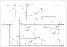
version 2
ok, ive taken onboard most of the suggestions. The next part of this project is to show the effects of negative feedback providing a means to increase the open loop gain, effectively removing the NFB.
im planning on altering it to do this by cutting the connectio between R8 and (R10/R11/C13), altering R8 to 10K and shorting C4. also please note the RC network R26/C13. In theory this will work but im not sure how to calculate R26?
Si
Attachments
- Status
- This old topic is closed. If you want to reopen this topic, contact a moderator using the "Report Post" button.
- Home
- Amplifiers
- Solid State
- my first amp, please could someone check it???