Still not seeing it
Hi Andrew.
I still seem to be missing something here. Leach's site states "With power supply voltages of about 58 V dc (+ and -), the amplifier will put out an average sine wave power of 120 watts per channel with an 8 ohm load"
Now as I calculate it 58 / 62 is about a 6% increase. If you apply that factor to the wattage you get 128Watts. This seems to lock up exactly with what was measured.
Are you saying that this version of the Leach amp is somehow alot more efficient that the original? As compared to the 110 Watts quoted for 50V unloaded supply - is the original leach simply horribly ineffeciant?
AndrewT said:Hi Byrd,
I am using a spreadsheet designed by Bensen to predict the output power and drive currents and looks at inductive loads relative to the temp derated SOAR.
I have tested a smaller amp running on 50.5Vdc rails unloaded that can output 110w into 8r and 200w into 4r continuous sine wave drive using only one pair of 150w output transistors. these results check out closely with the spreadsheet prediction.
I am surprised that you are showing 128w inro 8r on 62Vdc loaded rails. This peak output voltage is very low indicating to me that a lot of voltage is being lost somewhere. You should be getting at least 150w and maybe nearer 200w on those rails. high Re and long thin wiring and long PCB tracks might be a clue.
Hi Andrew.
I still seem to be missing something here. Leach's site states "With power supply voltages of about 58 V dc (+ and -), the amplifier will put out an average sine wave power of 120 watts per channel with an 8 ohm load"
Now as I calculate it 58 / 62 is about a 6% increase. If you apply that factor to the wattage you get 128Watts. This seems to lock up exactly with what was measured.
Are you saying that this version of the Leach amp is somehow alot more efficient that the original? As compared to the 110 Watts quoted for 50V unloaded supply - is the original leach simply horribly ineffeciant?
Hi,
the proportional increase in power due to higher supply rails does not predict accurately.
Firstly, the Leach quoted Vrail=58Vdc is, I think, the unloaded rail voltage. The loaded Vrail=55.2Vdc but this will depend on the VA rating and the regulation of the chosen transformer.
Secondly, The voltage losses through the output stage to the load will stay similar for small changes in Vrail.
Thirdly, the output power varies as the square on the effective supply voltage.
Fourthly, the Leach had 2 pairs of output devices, the smaller Leach clone has 3 pairs, Lgreen has 4 pairs and the original Leach clone has 5 pairs. With each extra pair of devices the voltage lost is reduced due to current sharing and one of the biggest savings comes from reduced Re of multiple pairs.
Fifthly, adequate smoothing capacitors increases the usefull DC available to give maximum utilisation after deducting the ripple from the loaded rail voltage.
All these indicate that a Leach clone could, with carefull attention to layout and component selection, produce about 150w into 8ohms from a 40Vac transformer. There is nothing wrong with Leach in general bar the lost voltage due to triple current gain stages in the output EF stage. My comparison was for a Sziklai connected predriver with discrete darlington as driver and output device which has inherently greater efficiency if driven from a common set of supply rails. My assumptions are based on a supply rail voltage to the driver and output device only and adequate drive to the predriver and voltage amp stage to allow the final current stage to deliver. I have no way of estimating what distortion is produced at these levels nor how the distortion might increase with reducing load values but I suspect the values I am quoting would be more indicative of the level to be achieved at just BEFORE the onset of very mild clipping on a scope view of the output voltage.
Finally a quick check on my calculator allowing a voltage loss of 5V from both your 65Vdc and 55.2Vdc gives 120w rising to 171w not 128w ((65-5/55.2-5))^2*120=171). However this is only +1.5db so are we discussing triviallities and/or should we await real testing?
Andrew I agree - enough theory - it is so impractical ")
Also I apologize if I have offended you - It was not intentional - just trying to learn. When something doesn't make sense to me I question it. I have seen how Jens was haranged in a couple of the earlier postings of this thread and should have recognised it in my own writing before posting.
Thank you for all your input into this project Jens.
still4given said:Hi Guys,
I've got a question.
The signal in has two separate inputs. One is routed through C6 & C7 and the other bypasses them. What is the reason for this? Which one should be used?
Thanks, Terry
Hi,
these inputs give us options, one is ac coupled, if we are not sure of the preamp that will feed the amp, it is wise to use this option, however, it we want a response down to 0hz the direct coupled input is available. very nice for jens to provide these options.
tony
15000uF capacitors
Hey there,
I am considering a Leach clone and am now choosing parts. I post this in this thread because I think I saw a couple of boards with the following:
15000uF, 80V electrolytic capacitor from Cornell Dubilier sold by JEA Capacitors on Ebay. The Ebay site described the dimensions as 35mm X 60mm. If anyone has these, can you please tell me if they are indeed 60mm in length? CDE's website don't show any 15000uF 80V caps in 35X60 but 35X80.
Thanks in advance. I'm aiming for a compact design hence the question.
15mF 80V caps
Hi,
I'm not at home so can't answer your height question but those caps do fit the board with lots of space around them. They are the same height and diameter as the 10mF 80V.
They are also the highest item on the board by far, so internal layout is determined by these.
Hi,
I'm not at home so can't answer your height question but those caps do fit the board with lots of space around them. They are the same height and diameter as the 10mF 80V.
They are also the highest item on the board by far, so internal layout is determined by these.
When buying caps of unknown age, or for general procedure, you should reform them.
Here are some links about reforming:
http://www.vmars.org.uk/capacitor_reforming.htm
http://home.insightbb.com/~stephenwmoore/Electronics/Reform.htm
http://www.chemi-con.com/guide/pg10.php
Here are some links about reforming:
http://www.vmars.org.uk/capacitor_reforming.htm
http://home.insightbb.com/~stephenwmoore/Electronics/Reform.htm
http://www.chemi-con.com/guide/pg10.php
pooge said:When buying caps of unknown age, or for general procedure, you should reform them.
Here are some links about reforming:
http://www.vmars.org.uk/capacitor_reforming.htm
http://home.insightbb.com/~stephenwmoore/Electronics/Reform.htm
http://www.chemi-con.com/guide/pg10.php
good info!

\Jens
Re: 15000uF capacitors
They are the ones I used. They measure 2 3/8" tall.
Blessings, Terry
Arius said:Hey there,
I am considering a Leach clone and am now choosing parts. I post this in this thread because I think I saw a couple of boards with the following:
15000uF, 80V electrolytic capacitor from Cornell Dubilier sold by JEA Capacitors on Ebay. The Ebay site described the dimensions as 35mm X 60mm. If anyone has these, can you please tell me if they are indeed 60mm in length? CDE's website don't show any 15000uF 80V caps in 35X60 but 35X80.
Thanks in advance. I'm aiming for a compact design hence the question.
They are the ones I used. They measure 2 3/8" tall.
Blessings, Terry
Hi Guys,
I am testing my boards and I have the bias set to 100mA and it seems pretty stable but I am reading about 350mV DC offset. Any ideas as to why I'm seeing so much. Is there something I can do to correct this? I don't have any resistors installed for R68 & R69. Could this have a baring on this?
I get anywhere from 12.0mV to 17.0mV across the emitter resistors. Each one is a little different.
Thanks, Terry
Hello Terry,
Thanks for the pictures of the CDE caps in your previous post. It confirms that they are indeed 60mm tall. Just surprised as I didn't see any product with that size at CDE's website.
About your most recent post, 350mV is definitely excessive and I doubt the lack of R68 and R69 is responsible for that. On the other hand, R68 and R69 appears to be totally unnecessary. Before I continue, let me state that I don't have a Leach amplifier so anyone can choose to ignore what I say below.
1) DC offset measurement is made without any input connected and no load at the output. Just checking to be sure.
2) I'd check the input differential pairs. Any current imbalance usually leads to output DC offset. Specifically check that R2=R21, R5=R20.
3) Check voltages at base of T1 and T6 are equal.
Post what you measure. Maybe someone else here may have more suggestions.
Good luck.
As for the offset, did you match the front end transistors?
If you did not, then the answer is probably there.
http://users.ece.gatech.edu/~mleach/lowtim/part2.html
The added benefit is also that the amp produces lower disortion. So some matching and "ugh" desoldering might be called for.
If you did not, then the answer is probably there.
http://users.ece.gatech.edu/~mleach/lowtim/part2.html
The added benefit is also that the amp produces lower disortion. So some matching and "ugh" desoldering might be called for.
Some good news. The second board reads fine.
Now to the bad one.
T1 C=65.5V B=39.6 E=39.0
T6 C=-66.0 B=-24.5 E=-23.9
R21 = -67.5,-66.1
R2 = +67.3, +65.7
R20= -24.6, - 1.059
R5= +39.6, +.0978
On the good board, The numbers aren't exactly the same side to side but very close. It reads 8.1 mV offset
Any ideas what may be causing the disparity?
Thanks, Terry
Hmm, it looks like D3 or D3 is bad/wrong value. Try replacing them.
The theory is D3+D4 provides a -40V reference voltage for the input pair. Likewise, D1+D2 provides +40V.
I would worry about matching transistors last. Like Dr. Leach said, offset won't go way off if matching is not performed.
Try focusing on D3+D4 first. Best of luck.
The theory is D3+D4 provides a -40V reference voltage for the input pair. Likewise, D1+D2 provides +40V.
I would worry about matching transistors last. Like Dr. Leach said, offset won't go way off if matching is not performed.
Try focusing on D3+D4 first. Best of luck.
Hi Arius,
Thanks so much. That makes perfect sense. I did try to match all of the transistors. The base voltages for T1 & T6 on the good board were both 39/-39. I can see where the zeners are not doing their job on this board. I will replace them I see what I get.
Blessings, Terry
Thanks so much. That makes perfect sense. I did try to match all of the transistors. The base voltages for T1 & T6 on the good board were both 39/-39. I can see where the zeners are not doing their job on this board. I will replace them I see what I get.
Blessings, Terry
Terry,
If you use 1% resistors and unmatched transistors you should be able to get less than +-30 to 40 mV on the output. If you use matched transistors you will be able to get an even smaller DC voltage.
I never bother with matching the transistors but use 1% resistors, by the looks of it you have used 5% resistors is this correct?
BTW 5% resistors may be ok if they are from the same batch as these tend to be close in value (but up to 5% more or less than the specified value)
Please keep us updated
\Jens
Terry, make sure the orientation of the diodes is OK. Also, look for solder bridges. These can be really aggrivating to find, because they can look like normal traces. Sometimes when you lift the iron, solder will flip off the iron and land in the wrong place, bridging the wrong traces or pads. Since you have a working board, lay the boards side by side and check that the orientation of all the components is the same on each, and compare ALL of the solder pads to see if they are identical as far as the position of the solder on them.
If you find a solder bridge and correct it, you may also find that a small signal transistor is burned out somewhere due to a short. So look for errors that may have caused a defective component first, so that when you replace a defective component, you don't fry it again.
If you find a solder bridge and correct it, you may also find that a small signal transistor is burned out somewhere due to a short. So look for errors that may have caused a defective component first, so that when you replace a defective component, you don't fry it again.
Hey friends,
Thanks so much for all of the help. She is up and running. It was one of the zeners. It only read 8.2 ohm and the others read 29. I didn't have any of the same manufacture but had other 20v zeners so I had to change them all out to get a good match. Boy do I hate changing parts out on a board with through plated holes.
I spent all day today mounting everything in the case. Started it up through my variac and a light bulb. Everything went well so I plugged her into the wall and away we went.
Man this thing sounds great!!!!
I don't know if its the regulation or just great design but this amp really kicks. I am very happy, can you tell?
The Hafler transformer doesn't seem to lack anything. I had the amp way louder than I care to listen to into 8 ohms and 4 ohms and I couldn't hear any sign of it flubbing out. Maybe you might see something on a scope but to my ears it is fine.
Thanks Jens for taking all the time to put this board together for us. It is a thing of beauty and goes together really well.
By the way. I used mostly metal film resistors which are 1% for the most part. Now that I have replaced the zeners I'm getting 0.2mV offset on one channel and 0.8mV on the other. Can't complain about that.
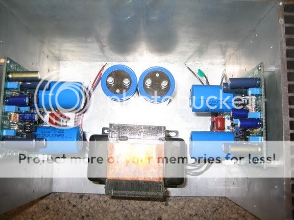
Here are some pics.
As you can see it got a little crowded inside.
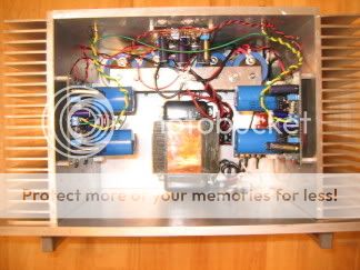

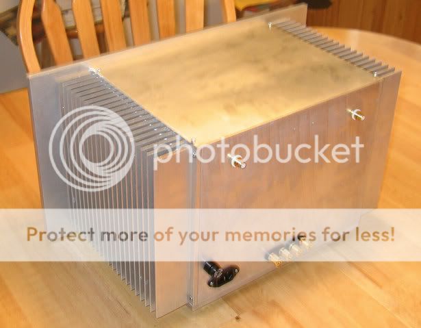

Blessings, Terry
Thanks so much for all of the help. She is up and running. It was one of the zeners. It only read 8.2 ohm and the others read 29. I didn't have any of the same manufacture but had other 20v zeners so I had to change them all out to get a good match. Boy do I hate changing parts out on a board with through plated holes.
I spent all day today mounting everything in the case. Started it up through my variac and a light bulb. Everything went well so I plugged her into the wall and away we went.
Man this thing sounds great!!!!
I don't know if its the regulation or just great design but this amp really kicks. I am very happy, can you tell?
The Hafler transformer doesn't seem to lack anything. I had the amp way louder than I care to listen to into 8 ohms and 4 ohms and I couldn't hear any sign of it flubbing out. Maybe you might see something on a scope but to my ears it is fine.
Thanks Jens for taking all the time to put this board together for us. It is a thing of beauty and goes together really well.
By the way. I used mostly metal film resistors which are 1% for the most part. Now that I have replaced the zeners I'm getting 0.2mV offset on one channel and 0.8mV on the other. Can't complain about that.
Here are some pics.
As you can see it got a little crowded inside.
Blessings, Terry
- Status
- This old topic is closed. If you want to reopen this topic, contact a moderator using the "Report Post" button.
- Home
- Amplifiers
- Solid State
- Smaller Leach Amp V1