A question about pcb layout came up in a thread called ”mos-fet amplifier question...”
I make my own PCBs but only a few of them are audioamps and I'm doubtful that any of them would pass ”OK” if an closer examination was made by an expert in this area.
This subject has been more or less discussed earlier on diyaudio with comments about groundloops, oscillation, noise and of course pictures on some real nice PCBs.
My thought is that ”PCB routing for audioamps” would end up in some sort of guide on how to, don't do this and why?
Anyone out there willing to propose or even better contribute with schematics on two amps. I think that two schematics with a small number of components, just enough to walk through the biggest traps.
I think one schematic of each BJT and MOSFET amp.
I would be happy if as many as possible on DIY could show up their artworks from the two schematics and then discuss what's wrong. Remember, this is in no way any sort of competition any layout is welcome.
Books has been written on almost any subject which comes up on DIY so why not PCBs.
If someone think this subject has been discussed enough let me know.
If something is unclear just ask, I'm just a Swedish guy so some words could be mixed")
Bjorn
I make my own PCBs but only a few of them are audioamps and I'm doubtful that any of them would pass ”OK” if an closer examination was made by an expert in this area.
This subject has been more or less discussed earlier on diyaudio with comments about groundloops, oscillation, noise and of course pictures on some real nice PCBs.
My thought is that ”PCB routing for audioamps” would end up in some sort of guide on how to, don't do this and why?
Anyone out there willing to propose or even better contribute with schematics on two amps. I think that two schematics with a small number of components, just enough to walk through the biggest traps.
I think one schematic of each BJT and MOSFET amp.
I would be happy if as many as possible on DIY could show up their artworks from the two schematics and then discuss what's wrong. Remember, this is in no way any sort of competition any layout is welcome.
Books has been written on almost any subject which comes up on DIY so why not PCBs.
If someone think this subject has been discussed enough let me know.
If something is unclear just ask, I'm just a Swedish guy so some words could be mixed
Bjorn
Hello,
I think that plated double sided boards are the way to go.
I have made several layouts of poweramps and found little difference to the sound (Same parts and schematics) if just some basic rules are used.
1) Lots of CU for powertracks
2) Lots of CU for ground
3) Seperate small signal ground
4) On board rail caps to minimise inductance in rails
5) Short tracks are made possible by using two layers
I can give my leach amp as an eksample:
\Jens
I think that plated double sided boards are the way to go.
I have made several layouts of poweramps and found little difference to the sound (Same parts and schematics) if just some basic rules are used.
1) Lots of CU for powertracks
2) Lots of CU for ground
3) Seperate small signal ground
4) On board rail caps to minimise inductance in rails
5) Short tracks are made possible by using two layers
I can give my leach amp as an eksample:
An externally hosted image should be here but it was not working when we last tested it.
An externally hosted image should be here but it was not working when we last tested it.
\Jens
Good information on PCB layouts is quite hard to find. There are a couple of good books out there on the subject, but I'm afraid I cannot recall the titles. I have never found any websites with anything more than basic information on them (except info on RF PCBs, but that's moslty not applicable to audio).
A few tips I have picked up:
A few tips I have picked up:
- Be aware of what components produce heat and keep them away from anything sensitive. try to keep hot components at the top of the board for best cooling. Tracks carrying high current will produce some heat too. Too much heat can warp tracks, so it can be a good idea to raise hot components off the board a bit, which also helps airflow around them, but longer leads mean more inductance.
- Use a ground plane if possible. If not, try routing power tracks on top of ground tracks to couple them capacitively. If you've only got a single-sided board then the best you can do is place them side by side.
- Use a double-sided PCB. They allow you to make much tighter layouts. SMT components help too, but they can be hard to work with by hand.
- Use star grounding. It also helps to keep signal and power grounds separated all the way to the PSU, i.e. use two ground connections to the PCB.
- Don't route noisy tracks close to signal tracks. Place a ground between them if they really have to be close.
- Supply bypass capacitors should be as close as possible to the circuit with as little inductance in the ground return as possible. SMT capacitors are very good for this as they can be placed between pins of ICs.
- Increasing track thickness decreases resistance but does nothing for inductance. To reduce inductance run multiple tracks in parallel and keep tracks short.
- Don't trust software to autoroute for you. The best it will do is connect the right points together, but otherwise it will be far from optimal.
The most important think I've found is to keep the output section on one end of the PCB and the input on the other. Even a little empty space in between is helpful. The reason is simple - the higher currents and voltages of the output signal can be picked up inductively by the lower voltage and current input traces resulting in oscillations. This is the same reason you shield input wiring or at least keep it as far away from the output as you can. You can usually combine this consideration with the the way you want to arrange the PCB/output devices/heatsink structur.
Have a sense fot what parts of the power rail traces will carry higher currents and be sure the are large enough. See www.vutrax.co.uk/trackwidth.htm for a table of track widths and note that thicker copper is also an option. While I also try to use nice wide tracks for ground traces, I've found no advantage to a ground fill. Some have reported it is prove to become an antenna! I try instead to keep the ground traces fairly short and take them off the board with an orthagonal wire ASAP. Look in the articles archive at www.rane.com there is a POwer Point presentation that mostly concerns digital circuits but has some interesting thoughts such as how a ground plane parrallel to the bottom or side enclosure can form a resonant RF cavity. This is pretty esoteric but some linear devices have pretty high ft's so this could be a another contributor to oscillation.
I had independently reach the same conclusion as the Rane presenter in on other area -- narrow traces are not all bad. In the small signal section I use narrower traces because what goes along with them is more space in between traces.
Other rules: avoid long straigt traces as they become antennas, juast putting an extra bend in here and there helps; avoid parrallel traces unless they are signal and return path, includinf traces on opposite sides of the PBC, per the ubiquitous D.Self, output sections are fairly imuse to ripple so I locate rail bypass caps closer to the small signal sections where they are most needed, usualy at the point the low and high current sections separate.
You may realize by now that there are no cookie cutter rules in this, just a lot of advice some of which is contradictory. That's one thing about the Rane articles mentioned -- you realize that even the pros have diffuculties and ambiguities in this area.
Upupa Epops said:To Jens : Are this big caps BESIDE rails fuses ?
Yes, another habit of mine, I ALWAYS use fuses on every channel in an amp. This is just for extra safety, but I like to be sure that there is something protecting the amp and/or speakers, should something bad happen somewhere.
\Jens
I did not read one very important rule yet:
Do not have signal traces leading to high ohm resistors parallel to another signal trace.
That is one sure way of getting an amplifier circuit to oscillate.
Avoid it, otherwise place a ground trace inbetween.
Preferably no 90 degree cornering, unless you can chamfer it by making the trace wider at the corner section.
I think there is never enough ground plane. The longer the ground trace to ground centre the wider.
If you try to follow all these "rules", including mine, you will think an impossible task lies before you. If you try to rigorously obey all of them you will never get anything done. Just getting all the componts on the board and connected without useing too many wire jumpers is challenge enough.
I suggest you just locate the comonents that MUST be at the edge of the board first, then fill in the rest by keeping related comonents fairly near each other (you be able to do this perfectly!) and start routing. Expect to take a few trys at routing before you even make the board -- you will find you hasve trapped yourself so that the last couple of traces are impossible -- just start over. Don't be frustrated - treat it as learning and practice -- when you finally etch the board it will be better just because you made several trial routings first.
Since the chances are high there will be a problem with the first etched board. Don't be afraid of cutting traces and re-routing with a bit of wire on the bottom side. Electrons don't care whether the board is pretty or ugly. And you will learn something from working out the problem.
Don't clip off the leads of the expensive devices too short until you know the board works. This lets you salvage the expensive stuff and makes it psychologically easier to throw out a PCB and start over.
Generalizing again
There are a couple of problems with the rules that were posted.
A- Almost anything you do to make one thing "better" makes something else "worse".
B- Some rules pertain to certain situations but do not apply to the immedeate situation. They have been passed on from person to person out of context. Possibly the biggest source for this is rules that come from RF and military practice. In fact, as an amp builder one thing you are always fighting is stray RF getting into your circuit, thus practices that facilitate good RF circuits may be exactly the opposite of what you need.
C- It's really hard to change just one thing on a PCB, and therefore establishing a clear cause-effect relationship is often hard. It's hard even when making a deliberate experiment. It's harder still to figure out retroactively, as when you re-rout the same troublesome circuit and suddenly it works. You may be able to identify 5 things you changed - but which one was critical ? One makes the best guess one can and passes the guess (opinion) on to another person. Baybe it's right, maybe not.
Thanks for all replies!
Excellent pcb Jens!
Very symetrical, guess that a double sided board play a big role and that you spent some hours to make the final finish, real nice artwork. Bad thing with double sided board for most hobbyist is that it is a bit tricky to make them. Does your amp get less noisy by using a groundplane like the one on your board?
Good points you've made 1-5 they are already added to my library
Thanks MR Evil for reply.
I've searched the web for books and hints and nothing useful came up, the book I found was written for Eagle cad, it seemed to me like a good choise but when I read the reviews I realized that it was more or less focused on the cad software itself. So if anyone can suggest a good book let me know.
Rest of your post contain many interesting points which has been memorized.
I've been into repair bussines for a long time and I've seen lots of misstakes whish ended up in burned PCBs and dried out electrolytic caps mounted close by hot high wattage resistors and lots of other failures.
Mr Evil what is the main reason to run the power traces on top of ground tracks or ground plane? I know that there will be some picofarads depending on trace width and type of board but for low frequency it will have little decoupling effect or is it for another purpose? Rf?
I seldom use the autorouter. I use the autorouter only when I'm tired and got all components were I want them to be then I run the autoruter just to see an uggly preview
It take it's time to write in English hopefully I'll speed up as a member at DiyAudio.
I'm home from work and not in good shape so I will have to take som rest but I'll be back tomorrow to continue this.
Bjorn
Excellent pcb Jens!
Very symetrical, guess that a double sided board play a big role and that you spent some hours to make the final finish, real nice artwork. Bad thing with double sided board for most hobbyist is that it is a bit tricky to make them. Does your amp get less noisy by using a groundplane like the one on your board?
Good points you've made 1-5 they are already added to my library
Thanks MR Evil for reply.
I've searched the web for books and hints and nothing useful came up, the book I found was written for Eagle cad, it seemed to me like a good choise but when I read the reviews I realized that it was more or less focused on the cad software itself. So if anyone can suggest a good book let me know.
Rest of your post contain many interesting points which has been memorized.
I've been into repair bussines for a long time and I've seen lots of misstakes whish ended up in burned PCBs and dried out electrolytic caps mounted close by hot high wattage resistors and lots of other failures.
Mr Evil what is the main reason to run the power traces on top of ground tracks or ground plane? I know that there will be some picofarads depending on trace width and type of board but for low frequency it will have little decoupling effect or is it for another purpose? Rf?
I seldom use the autorouter. I use the autorouter only when I'm tired and got all components were I want them to be then I run the autoruter just to see an uggly preview
It take it's time to write in English
hopefully I'll speed up as a member at DiyAudio.I'm home from work and not in good shape so I will have to take som rest but I'll be back tomorrow to continue this.
Bjorn
sam9 said:The most important think I've found is to keep the output section on one end of the PCB and the input on the other.
Even a little empty space in between is helpful.
Good stuff!

I think Pavel used the wrong word. I think he ment if you had the fuses before the big caps => easy to break the fuses when the power is switch on. I have done the same thing in my QRP02 Gainclone, fuses first then the rest. Somehow I think it feels better to have the fuses as the first part but still I see the problem with that.JensRasmussen said:
Yes, another habit of mine, I ALWAYS use fuses on every channel in an amp. This is just for extra safety, but I like to be sure that there is something protecting the amp and/or speakers, should something bad happen somewhere.
\Jens
BTW, Jens: A very nice pcb job!

Well I think that designing/choosing fuses is challenging in it self.
With 5 parallel output transistors and rails of about 68V the fuses have to be big, say (68-6)/4 = 15A, but on the other hand you want the fuses to offer some protection, so I think the fuses will need to be 10A slow blow types.
This size fuse will survive the surge current in the caps. I have used this for over a year on my prototypes. I remotely turn my amp on maybe 5 – 10 times every day, and have found no problem with fuses blowing.
The caps I placed on the board is only local decoupling, I have a central capacitor bank in the amp, where I keep 30.000µF for each rail. The only fuse I have before these is the fuse on the primary side of the transformer. The reason being that the current charging this much capacity will blow a 20A fuse quite often. I think it’s better to have a smaller fuse on the primary side of the transformer. The primary fuse is a major requirement anywas.
I also use a slow start circuit to limit the inrush current.
\Jens
sam9 said:The most important think I've found is to keep the output section on one end of the PCB and the input on the other.
Better still: Use completely independent PCBs for output stage, together with its power supplies+protection circuits, and another PCB (made as compact as possible!) for the voltage gain cell with it's power supply. (i.e: independent bridge+reservoir caps.)
All grounds returned independently to star point of course...
You may still take a further step and shield the entire output stage PCB, (including it's supplies alias: output stage bridge+reservoir caps.) a la Halcro!
SM2GXN said:
Mr Evil what is the main reason to run the power traces on top of ground tracks or ground plane? I know that there will be some picofarads depending on trace width and type of board but for low frequency it will have little decoupling effect or is it for another purpose? Rf?
If the return path for the current going through a trace is close by the inductance of the trace is lowered.
Halcro...Now...that is what i call a proper output inductor!!!
Are you shure it's not really for distilling moonshine?
quote:
Originally posted by SM2GXN
Mr Evil what is the main reason to run the power traces on top of ground tracks or ground plane? I know that there will be some picofarads depending on trace width and type of board but for low frequency it will have little decoupling effect or is it for another purpose? Rf?
If the return path for the current going through a trace is close by the inductance of the trace is lowered.
An example of the classic dilemma. What is good practice in one case introduces other problems in a second case. In some circuits, following the rule requires you to route one or the other trace over a much longer and convoluted path than would otherwise be necessay.
A "solution" I once saw in a comercial product was to form a "Y" in the off board wiring and bring DC power onto the at two independant points for each polarity. This was with a two layer board so I think it was a deliberate strategy to keep the power traces on the board as short as possible. I've also seen something similar done to tie two parts of the ground together from distant parts of the PCB - in this case a solid core wire exites/entered the PCB at each end and formed a brich about 1/2 above the board. This one as well looked laike a deliberate strategy and not a "hack".
The nice thing about this is that it shows there is room for creative solutions, which offers some consolation for the absence of clear unversally applicable rules.
mikeks said:Better still: Use completely independent PCBs for output stage, together with its power supplies+protection circuits, and another PCB (made as compact as possible!) for the voltage gain cell with it's power supply.
Mike,
you think that is always superior to a 1-board solution ?
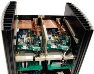
What is the light stuff on the outside of the Halcro heatsinks?
(i adore chimney heatsinks)
(did anyone ask who the goodlooking on Mike's avitar is yet? )
Halcro...Now...that is what i call a proper output inductor!!!
"Almost" as big as the coils in my RF amplifiers!If you try to follow all these "rules", including mine, you will think an impossible task lies before you. If you try to rigorously obey all of them you will never get anything done. Just getting all the components on the board and connected without useing too many wire jumpers is challenge enough.
You may realize by now that there are no cookie cutter rules in this, just a lot of advice some of which is contradictory. That's one thing about the Rane articles mentioned -- you realize that even the pros have diffuculties and ambiguities in this area.
Thank you sam9 your posts has been real interesting reading, Have you ever thought about writing a book
Because of those ambiguities it makes it hard to belive all you read and you shouldn't "that's what I've learned my kids". Internet is excellent but the fact is that it could even change the history if you are not able to interpret all information you read
If the return path for the current going through a trace is close by the inductance of the trace is lowered.
Thank you relder for explaning, I didn't think of that but now I know it's a good way to lower the inductance by doing so.
I was about to start routing a board on one of Anthony Holton's Lateral FET amps but then I was caught by a real bad cold.
I don't know if I got to have Anthony's permission to put the board on Diy? He makes his living on doing all those amps so it might be better to ask.
Bjorn
First, I try to be aware of:
- where some components (or mounting holes) *must* be placed
- where currents flow
- hierarchy of perturbators to victims (high to low dI/dt, high to low dV/dt) => gives good indications of where tracks should be the shortest, and which components/tracks to keep apart
- card to case coupling
- how much current flow from grounds to supply (or other card)
Second, I place&route with all that stuff in mind, with normal track width
Third, I refine (or redo), taking into account:
- min/max voltage of each net => constraint on track to track spacing (12.5mil between +/-35V rails is not enough for my taste, for example)
- hot spots (components suceptible to heat, track heating due to high currents) => for "how wide" a track/copper pour, and "how wide" the spacing around some components.
- how RF may arrive and depart from card
- how to benefit from coupling rather than fight it (ex: no problem to keep close 2 tracks that are already bonded by a cap)
Fourth, I try to adapt the schematic in order to make things easier. Sometimes, it can help to split a resistor in two, and/or move a component to another board.
Fifth, I sleep on it, then slap my face because I realize I've missed something, and rework the lot
My 2 cents...
- Status
- This old topic is closed. If you want to reopen this topic, contact a moderator using the "Report Post" button.
- Home
- Amplifiers
- Solid State
- PCB routing for audioamps