Hi All,
In place of 50W, please read 200W.
The darned thing works, and has so much transient attack it is near unbelievable.
Presently running on only 46 Volts and with more than enough reserve. I will be going to at least 50V though, because my aim has always been to match the power of a current dumper, but with the finesse of a JLH.
Any triers ? Destroyer built one of my earlier versions in a day and had it running, but he has moved over to class-D.
This amplifier is for use with loudspeakers that are designed for low amplifier impedance driving; the sound will be quite different if driving loudspeakers that have been optimised with higher impedance or long cable drive unless a similarly long cable is retained, but then that will ruin some of the directness this amplifier promotes.
The differential tail filter now introduces a slight power-up thump, not a problem but no longer silent. Actually it is reassuring, though I prefer completely silent because there is no hum or hiss either.
Cheers for now ............ Graham.
Attachments

Is this for the VAS and outputstage that blend into 1?for the uniquely elegant twist in the topology.

In tube terms, that's called a "split load" phase splitter. The design is ancient...probably came down out of the trees when we went from dragging knuckles to walking upright.
As to why you don't see it in more solid state stuff, I dunno. There are scads of things that the tube guys did that never got ported over to solid state.
The upside is that you're guaranteed a perfect split. The downside is that the Zout off the plate/collector/drain is waaaay higher than the cathode/emitter/source. In some circuits that impedance mismatch can cause problems. I've seen at least one commentator who favored putting both halves of the signal through followers in order to even out the Zout, but then you've added another device into the signal path...
Without further scrutiny, I'm not clear as to why there's a small resistor above the collector load R...the classic split load has identical resistance above and below the tube. If I get time, I'll stare at the thing for a while later. I'm sure there's something obvious that will jump out at me.
Grey
Originally posted by GRollins
As to why you don't see it in more solid state stuff, I dunno. There are scads of things that the tube guys did that never got ported over to solid state.
Like chokes - which is kind of funny because they are much better suited to a low impedance environment
The downside is that the Zout off the plate/collector/drain is waaaay higher than the cathode/emitter/source.
perhaps that's why in spice JLH give lower distortion with a darlington o/p device at the 'top' and a regular BJT at the 'bottom'
PS
the bias current for the 'bottom' tranny comes through the phase splitter tranny via...
the bias current for the top tranny comes through that extra resistor
thanks for that - I never understood quite like that before.
Hi,
Re split load phase inverter:
Sorry, that is not correct, but it is still debated in the tube community as it is not so easy to realise.
Given that the loads are equal the output impedance of anode and cathode are equal and actually lower than you would expect. Here is a document describing how the output impedance can be calculated. http://www.aikenamps.com/cathodyne.pdf
The most common mistake is to calculate output impedance from anode or cathode separetly which of course is perfectly alright if the circuit is not used as a phase splitter but assuming that both cathode an anode are loaded give a very different result.
Regards Hans
PS, I have built and measured output impedance and gain of many split load phase inverters and have by measurements confirmed that the calculations in Preismans document are indeed correct. One easy way to confirm this by oneself is to do a simulation in Spice. DS
Re split load phase inverter:
The downside is that the Zout off the plate/collector/drain is waaaay higher than the cathode/emitter/source.
Sorry, that is not correct, but it is still debated in the tube community as it is not so easy to realise.
Given that the loads are equal the output impedance of anode and cathode are equal and actually lower than you would expect. Here is a document describing how the output impedance can be calculated. http://www.aikenamps.com/cathodyne.pdf
The most common mistake is to calculate output impedance from anode or cathode separetly which of course is perfectly alright if the circuit is not used as a phase splitter but assuming that both cathode an anode are loaded give a very different result.
Regards Hans
PS, I have built and measured output impedance and gain of many split load phase inverters and have by measurements confirmed that the calculations in Preismans document are indeed correct. One easy way to confirm this by oneself is to do a simulation in Spice. DS
Hi David,
Its not really a VAS.
The phase splitter collector does act like a VAS for the upper output half, but the emitter is simultaneously current driving the lower output half in opposite fashion, and the driver collector/emitter should work into similar loads, dynamic as well as passive for low pre-NFB distortion.
The phase splitter needs to be a low capapacitance/high frequency device with good gain so that internal bias/charge currents do not upset the phase splitting balance at frequencies above audio, lest phase shifted re-combinations within the output stage create a current notch between halves that would lead to closed loop instability. This is one reason why output Mosfets cannot be simply dropped into the JLH class-A.
As I wrote, both output halves amplify separately but simultaneously. Also an impaired transduction response in one half does not immediately ruin NFB loop controlled linearity because the other half is still working.
Its not just a minimal number of stages that count either, but the type of stage; ie. whether CB, CC or CE and series or parallel that counts.
Output Mosfets can be used, but as Grey points out, the collector impedance at the driver is much higher and not capable of equally driving the gate capacitance of an upper device. There is also the aspect of Mosfet gate capacitance introducing what is effectively R-C delay; extra stabilisation immediately becomes necessary and this increases/degrades propagation/NFB delay. I'm not saying that Mosfets cannot be used in this amplifier, but the final characteristics will be quite different.
Hi Grey,
You hit on the very point that makes difficulties for the JLH - output stage drivers make stability worse ! This is why I have used such low value resistors in the output stage so that the circuit maintains full class-A control unless the output impedance demand has a momentarily and virtually self stabilising low impedance.
I still have concerns that there could be momentary instability, and thus I do not yet regard this circuit as being final. I might yet change or redistribute the 'C's fitted, or maybe will even ditch both BC557Cs unless their value is proven to be audibly worthwhile.
I might also dispense with the differential tail supply filter too because with this amplifier having a 1A quiescent current it actually runs very loudly before the rail currents start increasing, in fact it is much too loud for home use by the time the smoothed rails draw 2A and with modern supply components there is little rail voltage disturbance.
" - a small resistor above the collector load - " you might be noticing the bootstrapped upper half supply resistor - this to ensure that current drive to the upper output half does not become reduced as positive output swings increase.
Anyone tried simulating yet ?
The circuit is not perfect, especially with squarewaves, but then simulators do not include all of the series resistance/inductance and parallel capacitance losses which arise due to normal wiring. I do however already hear an excellent basis for a home constructed design that will satisfy me, where other supposedly near perfect designs have not.
I have not been feeling at all well recently, so whilst I can write up here, my hands-on progress with the amplifier is likely to be much slower than others could make. Thus I have been happy to report my findings but further developments are likely to be slow.
I see there are two more replies, but I must post this first.
Cheers .......... Graham.
Nelson Pass said:S**t, F**b, Z**k, and G**g!
Yet another secret that will never be told !
Graham,
Do you think that I can build this circuit as is without the risk of having to extensively modify it later? Iq of 1A is interesting and attractive.
I have two 500VA transformers with tappings of 30 and 35 volts on the secondary along with 180-200-230Volt tappings on the primary side. Perfect for this job, I suppose.
And what is the kind of heatsinking required?
Thanks.
Hi, Graham,
I begin to understand how this JLH type works. I haven't understand the capacitance requirements yet, but I think there is a drawback for using bipolar for this phase splitter. The equation for bipolars is IE=IC+IB, that means the I in emitor will never be the same with I in the collector for bipolars.
With tubes or FETs, Isource is exactly = Idrain. Can mosfets/fets used for this phase splitter to ensure equal drop on upper/lower drive?
Current flows in loops
Where does the gate/grid current flow?
With tubes or FETs, Isource is exactly = Idrain. Can mosfets/fets used for this phase splitter to ensure equal drop on upper/lower drive?
Where does the gate/grid current flow?
phase splitting isn't required to be that accurate - in fact even with perfectly matched spice output transistor models my sims show substantial asymmetry developing as the output Q operating points diverge as output I and V change
Graham's Class A/JLH output thread:
http://www.diyaudio.com/forums/showthread.php?s=&threadid=40355&highlight=
Graham's Class A/JLH output thread:
http://www.diyaudio.com/forums/showthread.php?s=&threadid=40355&highlight=
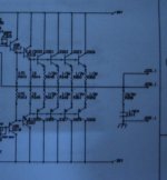
Further to my above posts and the last circuit.
The top 1k2 resistor runs hot and needs at least a 2.5 watt rating; don't burn yourself !!!
With the output bias current sinking mirrors connected as per the second circuit, the current splitting transistor still does not get hot. I am now using a 20 degrees C per watt dissipation clip, and it is only slightly warm.
Hi Mike,
The driver transistor splits the current passing through both of its series connected collector resistors as demanded by the output devices to set up a dc feedback loop controlled bias. When an upper Darlington is used almost all of the current passing through the driver collector resistors contributes towards biasing the lower device, whilst the relatively high collector resistance does not limit postive going output, as would be the case with a plain transistor.
Using the higher gain device of two in the upper position of a JLH original circuit is better for this reason.
The upper of the two collector resistors is merely part of the bootstrap ratio, which is optimally different with different output device types. No one golden ratio suits all circuits.
When the load is reactive the 'dynamic' output device base currents are not a simplistic split of this 'bias' current passing through the driver transistor collector resistor, which is why a standard JLH loses clarity when it is run above approximately half of the expected maximum listening power with a real world loudspeaker.
Hi Hans,
Oh how happy I would be if power bipolar and Mosfet devices had the same input characteristics as the grid of a pentode or tetrode; ie. near linear phase splitter loading.
When you connect a semiconductor to a split load phase invertor the only time it remains balanced is at minute signal level close to its quiescent biasing conditions.
Once the voltage starts swinging, the output devices conduct with base/gate charge/requirements that cyclically alternate in a manner whereby the upper resistor/driver transistor/lower resistor are obliged to cope with them whilst attempting on-going balanced drive operation.
All individual electrode impedance calculations are then out of the proverbial (operating) window, because, as you state, the circuit must be viewed as a whole. Long tailed pairs, VAS+CCS, and symmetrical drive are often used to overcome these single ended non-linearities.
With a thermionic pentode or tetrode running in class-A or AB1 the dynamic voltage/current requirements are relatively simple. Even the humble Miller C afflicted triode does not have grid induced linearity problems akin to semiconductors, which is why triodes can still provide a top class performance with appropriate drive.
The current flow between resistor/collector and upper output device, and between emitter/resistor and lower device have a variable impedance relationship resulting in non-linear current flow, due to the semiconductor action of the output devices modifying activity of the split load driver. There is a cyclic impedance variation about nominally equal values, but it does not remain equal. Impedance can be high positive going at the collector, but then high negative going at the emitter, and this is what sets natural circuit limitations. This is what I refer to as high collector impedance, because it is this that causes asymmetrical output and slew limits.
This also is the reason for a JLH simulation becoming increasingly asymmetrical with increasing output load voltage amplitude and increasing frequency, and is my reason for using one additional current mirror per output half to inversely provide additional impedance reducing current load for both collector and emitter current drives, these act separately, but equally and oppositely, to provide a fractional drive compensating release that functionally extends peak NFB loop controlled balanced driving capabilities.
I have used several different (balanced) driver current loads in the past in repeated attempts to accomplish this, but the last circuit above is the first one that works properly without increasing distortion.
So it is the high series resistance driving impedance at the collector of the current splitter that is the limiting factor for the JLH output stage, and ensuring an equivalent emitter resistance does not help at higher amplitudes and frequencies. Fitting the upper Darlington is not an ideal solution either because the current splitting driver then no longer works linearly.
(Not lecturing anyone here Hans, just getting my findings down for readers to muse over.)
Hi Sam,
35V rectified would be approx 50V at the rails. This will not be found wanting.
The only thing you might need to change would be small Cs to cope with oscillation. Mine does not, but that is not something I can remotely guarantee.
My heatsink is 200mm long x 125mm wide with 40mm deep longitudinal fins and gentle low noise fan cooling.
Test the circuit board part first with a 9V battery connected between + and - rails and no output devices. Put a 10k resistor between +ve and ground, also connect driver collector to NFB return. LED should light, collector should go to approx 4.5V, current should be a few milliamps through 1k2 resistors. Check for correct bias around the mirrors. Then repeat with output devices connected and 10k removed.
Temporarily fit a 390 ohm resistor in series with the 220 bootstrap source resistor. Fit two 10 or 17W 22 ohm resistors one in series with each amplifier rail for first switch on. Power up with a 10 ohm load resistor. If voltages okay and amp is equally biased then connect up full power. Have an AM radio beside the amp but not tuned to a station. Any oscillation - then cure it. Take out the 390 resistor and see what rail current you get with the 220 ohm resistor, I would not go below 180 ohms even if the current does not manage 1Amp. Adjust or change the 220 ohm after an hour for 1A current, and trim the output zero.
Then you are ready to go.
Hi Lumanauw.
It is the capacitance of fets that concern me with this circuit. Also remember the driver V.ce (V.ds) must fall low for good negative drive, and that a warm bipolar driver introduces minimal imbalance anyway. I have checked this out with a deliberately selected low hfe BD139 which still worked well. The 2SC3421 has nicely low capacitance and good gain which makes for excellent current splitting.
Hi JCX,
Quite so !
Cheers .......... Graham.
Graham
combining classes of operation is nothing new and it is less uncommon that it seems
in fact many darlington outputs use a resistor from driver emitter to output bjt emitter. So drivers are kind of output devices in class A in a classic 'AB' output stage. Am I wrong?
combining classes of operation is nothing new and it is less uncommon that it seems
in fact many darlington outputs use a resistor from driver emitter to output bjt emitter. So drivers are kind of output devices in class A in a classic 'AB' output stage. Am I wrong?
I'm running on one to ten minute snatches of time. Last night I looked at the schematic, scanning for the phase splitter, found it, ran my eye vertically to verify resistances above and below (but not horizontally, hence missing the cap for the bootstrap), posted, and ran on to the next thing. Bootstrap, it is.
This is the first I've heard that the relative plate/cathode Zout of the split load phase splitter is "debated" in the tube community. Anyone who wants to argue symmetry or lack thereof in the Zout of split load phase splitters can have at it. I can barely find time to scratch, much less enough to waste arguing.
You can simulate till the cows come home, but won't know anything more than you did when you started. I gave up simulations years ago. They don't work. Hell, the first twenty pages or so of the Aleph-X thread are filled with various people telling me that their simulations were telling them it would never work. I knew better...I had the prototype running before I even started the thread. Reality trumps simulations every day of the week.
Grey
in fact many darlington outputs use a resistor from driver emitter to output bjt emitter. So drivers are kind of output devices in class A in a classic 'AB' output stage. Am I wrong?
Do you mean like this? The first driver has 470ohm to output. The second driver has 10ohm to output. The outputstage has 0.1ohm to output? Is this AB+B?
Attachments
I might be wrong here. Tubes and fets/mosfets doesn't suck current at their grid/gate?Where does the gate/grid current flow?
Graham Maynard wrote:
No problem, but actually my reply was in response to the comments by G Rollins on tube based phase splitters
G Rollins wrote:
I tend to agree with you, (about not finding enough time to argue) I have debated this issue in many forums but always meet people like yourself. Have you read the paper by Preisman? Have you measured output impedance and gain of a tube based phase splitter?
As I mentioned, (and as you conveniently ignored) I have confirmed the calculations in Preismans paper by real measurements, I have also done simulations and with my models the simulations give a result that is well in line with the practical result.
Regards Hans
(Not lecturing anyone here Hans, just getting my findings down for readers to muse over.)
No problem, but actually my reply was in response to the comments by G Rollins on tube based phase splitters
this has been proven wrong by many.The downside is that the Zout off the plate/collector/drain is waaaay higher than the cathode/emitter/source.
G Rollins wrote:
Anyone who wants to argue symmetry or lack thereof in the Zout of split load phase splitters can have at it. I can barely find time to scratch, much less enough to waste arguing.
I tend to agree with you, (about not finding enough time to argue) I have debated this issue in many forums but always meet people like yourself. Have you read the paper by Preisman? Have you measured output impedance and gain of a tube based phase splitter?
Tell that to people in the electronics industry where simulations today are an indispensible part of every day work, any company that dont use simulations are just not competetive. Simulations work well if the models and calculation methods are good enough, otherwise rubbish in rubbish out. The biggest problem for DIYers using simulations is that they dont have the experience needed to know if the result is reasonable or not, you can see a lot of that in this forum.You can simulate till the cows come home, but won't know anything more than you did when you started. I gave up simulations years ago. They don't work.
As I mentioned, (and as you conveniently ignored) I have confirmed the calculations in Preismans paper by real measurements, I have also done simulations and with my models the simulations give a result that is well in line with the practical result.
Regards Hans
- Status
- This old topic is closed. If you want to reopen this topic, contact a moderator using the "Report Post" button.
- Home
- Amplifiers
- Solid State
- Class-AABB output stage.