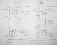
I made an experiment with CCS. The supply is +/-15V, and the reference for the CCS is 2xIN4148 drop=1V3.
In drawing I, all works fine, the A CCS gives 3.2mA to 1k load, and CCS B gives 6.95mA to 1k load. The current, voltages are measured, and nothing is unusual.
In drawing II, something strange is happening. Here I connected both CCS's with 1k load. The A CCS (the smaller one) still working fine, but CCS B doesn't work normally.
In the CCS B (of drawing II), the drop of the IN4148 only 1V2(from 1V3).
The current passing through 1k load is 3.2mA (exactly the same as the upper/smaller) CCS value. But the drop in 100ohm resistor of B CCS is 0V53, that means there is 5.3mA current here.
Also, the VBE of CCS B increasing to 0V67 (from 0V58).
If in CCS B, in the transistor, the collector has 3.2mA passing thru, but in the emitor there is 5.3mA passing thru, where is 2.1mA (5.3-3.2) coming from? Is it coming from base, that makes the drop of 2xIN4148 only 1V2?
A transistor can do this? Passing big current from base to emitors but not destroying the transistor itself?
1. The VBE figure seems doesn't relate with current passing from C to E. The current passing in VBE=0V67 can be less than when VBE is only 0V58
2. Or this happens because there is big current (2.1mA) passing from base to emitor junction?
Attachments
lumanauw,
I am a novice in electronics but I'll try (if I am wrong I can still learn !)
It looks like transistor B in circuit II is saturated. DC current gain is too low. The high base current explains the higher Vbe voltage as this B-E junction has a small resistance and therefore, Vbe drop increases with current too (just a little). Also, another consequence of a high base current is the decreased voltage drop in diodes).
Try to measure Vce of this transistor. If it is close to 0 then it is saturated.
Can you tell us which transistor are you using ?
Best regards,
João Pedro
lumanauw said:In drawing II, something strange is happening. Here I connected both CCS's with 1k load. The A CCS (the smaller one) still working fine, but CCS B doesn't work normally.
Hi,
Set current in both CCS on same value. CCS B transistor doesn't work in active operation area in your setup.
Regards,
Milan
What is "transistor saturating"? Is it very bad for audio reproduction? Is it the same when people talks about clipping?It looks like transistor B in circuit II is saturated
What makes DC current gain?DC current gain is too low
What condition makes the base draws so much current, but do not imply in collector current?
The transistors are BD139 and BD140.
Actually, I put these configuration on a purpose. I wanted to know what happens in CCS B.Set current in both CCS on same value. CCS B transistor doesn't work in active operation area in your setup.
Yes, It's very clear in the experiment result. But why is the lower CCS transistor not acting normally like ordinary transistor (HFE definition)? At first I really hope the lower CCS doesn't act like this.If you connect two current sources with different current in series, cross current will be given by current of lower current source.
I'm searching for a simple cct (transistor, R or dioda) that acts like a "minimal voltage limiter". That means if an input is injected to this simple cct, the voltage can rise, but if there is no input, or the input is negative (sucking) signal, the voltage can hold at a certain voltage (not dropping to 0 or turning negative). It has tobe adjustable too, not fixed like zener.
Hi lumanauw !
This looks like a typical situation of reversebiasing.
If a transistor does not "get rid" of the needed current
through the collector, it does through base.
Or in other words, you try to get a negative vce, which
is not possible. That's the saturation.
Unless you don't exceed the maxrating for basecurrent
given in the datasheet, the transistor does not get
destroyed.
In the case of reversebiasing a transistor does not
really work. This typically happens if an amplifier clips.
Mike
Upupa Epops said:If you connect two current sources with different current in series, cross current will be given by current of lower current source.
I follow Mr. Upupa Epops
")
lumanauw said:1. The VBE figure seems doesn't relate with current passing from C to E. The current passing in VBE=0V67 can be less than when VBE is only 0V58
No.
Don't forget the Ic of BJT is relate with the Vce...you should check the Vce,but maybe can not get the correct value of Vce in practice.
cheers.
X.G.
Re: Re: What happen with this transistor?
sorry,I take a mistake
I should say:the NPN tr works in saturation area,and the PNP works in line area,not like the left circuit which both of trs work in line area.their Vce is clearly different
X.G. said:
Don't forget the Ic of BJT is relate with the Vce...you should check the Vce,but maybe can not get the correct value of Vce in practice.
cheers.
X.G.
sorry,I take a mistake
I should say:the NPN tr works in saturation area,and the PNP works in line area,not like the left circuit which both of trs work in line area.their Vce is clearly different
lumanauw said:[snip]Yes, It's very clear in the experiment result. But why is the lower CCS transistor not acting normally like ordinary transistor (HFE definition)? At first I really hope the lower CCS doesn't act like this.
[snip]
You are setting the individual biases for a specific current through each transistor. These currents are not exactly the same, due to variations in the Vb and in the transistor gain. But, by connecting them together, you try to force them to have equal currents. So, something's got to give, it is impossible to have the same and different currents at the same time.
One transistor doesn't work in the linear mode anymore, and gets rid of the excess current the other one tries to force on it through reverse C-B current. That's also what MikeB says.
Saturation is when the Vce gets so low that the Vc gets below Vb, and it is impossible to get more current through the transistor by increasing the Ib or Vbe. Saturation is often used in transistors used as switches: at saturation, they have the least voltage loss, so can take a lot of current without overheating.
Clipping is similar, but from a different cause: The Ve goes up until it hits the supply, and the Vce becomes very small. One bad thing about saturation is that it takes the transistor a relatively long time to come out of it, because the Ib is really much to big for the Ic and all that base charge needs to be taken out first before the IC can start to drop.
That's why you often see low value resistors between B and E of drivers and output transistors: to get the base charge out quickly for fast recovery after clipping or other overdrive conditions.
Jan Didden
To put it another way:
CCS A supplies 3.27mA. That would give 0.327V across B:s emitter resistor. Add 0.6V Vbe, and there's 15-0.927 volts across the 4.7k base resistor. That will result in 3mA through that resistor. Where does that go? Well, there's clearly not enough voltage to forward bias the diodes, so the current has to run into the base of transistor B. Suddenly there's 6.27mA through the emitter resistor, and hence 0.627 volts across it. So now there's 13.873 volts across the 4.7k resistor. Repeat until convergence, and add that Vbe increases logarithmically with Ib, and your measured values make perfect sense.
Rune
runebivrin said:To put it another way:
CCS A supplies 3.27mA. That would give 0.327V across B:s emitter resistor. Add 0.6V Vbe, and there's 15-0.927 volts across the 4.7k base resistor. That will result in 3mA through that resistor. Where does that go? Well, there's clearly not enough voltage to forward bias the diodes, so the current has to run into the base of transistor B. Suddenly there's 6.27mA through the emitter resistor, and hence 0.627 volts across it. So now there's 13.873 volts across the 4.7k resistor. Repeat until convergence, and add that Vbe increases logarithmically with Ib, and your measured values make perfect sense.
Rune
Rune, you sound like Spice!
But you're right in my book.Jan Didden
lumanauw said:
.....
I'm searching for a simple cct (transistor, R or dioda) that acts like a "minimal voltage limiter". That means if an input is injected to this simple cct, the voltage can rise, but if there is no input, or the input is negative (sucking) signal, the voltage can hold at a certain voltage (not dropping to 0 or turning negative). It has tobe adjustable too, not fixed like zener.
Hi:
May be you are looking for something that works like this?
Attachments
janneman said:
Rune, you sound like Spice!
Jan Didden
That's me: The original Spice Boy!
Seriously, this reminds me of my first forays into transistor circuits, 30 years ago. I hadn't quite groked that they pretty much work like controlled current limiters. I thought the current somehow emanated from the transistor itself, so tried without collector voltage, with limited success...
Rune
If a transistor does not "get rid" of the needed current through the collector, it does through base.
One bad thing about saturation is that it takes the transistor a relatively long tme to come out of it, because the Ib is really much to big for the Ic and all that base charge needs to be taken out first before the IC can start to drop.
I get it now. If the collector cannot supply the current needed, it will suck from base. In audio amplifier cct, in what part this can happen (besides very high output like Janneman said)? Does it happen in turnon-turnoff/crossover distortion in class B/low biased AB?
Mosfets doesn't have base current mechanism. Is there anything similiar if the CCS A and B are built by mosfets?
Hi, Rodolfo,
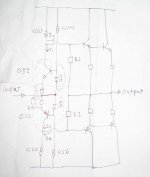
Actually I'm trying to make a non-turnoff (advoiding crossover distoriton) cct for push-pull EF output stage. Blomley uses certain topology, that cannot be implemented in ordinary EF output stage.
At first (before I know that CCS can acts weirdly), I'm thinking something like this.
I try to create a output/bias scheme that positive signal only rides positive side transistor (NPN) without disturbing at all the PNP, and negative signal only affects negative side transistor(PNP), without disturbing NPN at all. This way I hope with positive signal, the bias for negative transistor doesn't change/drop/dip at all (which ordinary VBE multiplier does).
Attachments
lumanauw said:I get it now. If the collector cannot supply the current needed, it will suck from base. In audio amplifier cct, in what part this can happen (besides very high output like Janneman said)? Does it happen in turnon-turnoff/crossover distortion in class B/low biased AB?[snip]
Saturation also happenss if you run your power amp full power at 20kHz and if you output transistors are not very fast (and mostly they aren't). The drop in IC of one transistor at the crossoverpoint is slower than the increase in Ic of the one that is taking over. The feedback tries to keep the signal correct, , so you end up with a lot of current going from V+ to V- without going to the load. Full power amp tests are often destructive, while saying nothing about the amp's ability to drive music signals into the speaker.
Jan Didden
lumanauw said:[snip]At first (before I know that CCS can acts weirdly), [snip]
Well, you're not being fair to the current source
.It's like putting 1 kg on one side of a balance and 2 kg on the other side and then complain that the balance is, err, out of balance.
Jan Didden
Well, you're not being fair to the current source. It's like putting 1 kg on one side of a balance and 2 kg on the other side and then complain that the balance is, err, out of balance.
I tought that a CCS is a "maximum current limiter". I tought that with 10mA CCS, I can pass 1 to 9mA without problem, but cannot pass 15 or 20mA.
The simple experiment shows that 10mA CCS if directed to pass only 5mA or 2mA will suck current from base. This is not in my tought at first.
If my assumption on CCS as a "maximum current limiter" works, then the CCT in post #17 will work as non-turnoff bias scheme like this:
I came up with this idea. The idea comes from my tought, that a CCS is a max current limiter. A CCS can be passed by a current lower than it's CCS value, but cannot be passed by current higher than it's CCS value.
In that drawing, the bias scheme CCS1 is formed by LED reference, a transistor, and an emitor resistor. So as CCS2. Between RE1 and RE2 there is parrarel VR for adjusting bias. This will adjust how many mA can be passed through these 2 CCS's.
The leds are powered by CCS4 and CCS6, due to full swing properties it will need CCS, cannot use R loading.
There is also CCS3 and CCS5. This makes the "folded cascode" level shifter.
The idea is like this. Lets see positive half first. CCS3 is giving constant current, lets say 20mA.
The bias adjustment will adjust how many mA can pass through CCS1+CCS2, in the form of I1. If I1 is 10mA, so I2 will be 20-10mA=10mA. This I2 goes to R1, makes a voltage drop on R1 that drives output NPN transistor.
If I1 decreasing, then I2 will increase, because CCS3 always forcing the same current value. We set CCS1+CCS2 to be 10mA.
The input point (audio signal) is coming to emitors of CCS1+CCS2. I assume the signal is in the form of current.
If the input is +5mA, then CCS1 will only pass 5mA, because CCS2 can only receive 10ma (preset before) and there is already 5mA from the input signal. Then I2 becomes 15mA.This will excite the NPN output to give positive signal output.
Because CCS2 is set for 10mA, this +5mA input will not go through CCS2, because CCS2 is already in its maximum limit (set at 10mA). This means I3 and I4 in lower section will always be the same, this also means the drop in R2 will always the same if the signal is positive (+ current coming thru the input).
So, because the input current is passing through 2 CCS, the positive input current will only disturb positive bias part, and not disturbing negative bias part. So as negative signal will only disturb negative part, not disturbing positive output stage part.
If my tought are correct, this should prevent non-turnoff in class AB power amp. But I don't have equipment to know if this idea will work.
Another possibility of this cct, is when we attached the center of the LEDS not to input, but connect it to output. It will change to perform EC. So if the center of the LEDS are connected to input it will perform non-turnoff, and if it's connected to output it will perform EC (But I think it cannot do both at the same time)
What do you think about this non-turnoff idea?
I've got another dumb question. If a transistor has HFE=50. This means if we put 1mA in the base, the Collector will have 50mA and Emitor will have 51mA.
If we reverse the condition, will the reverse situation occurs? If I push 50mA in the collector, will the base automaticly draws 1mA?
- Status
- This old topic is closed. If you want to reopen this topic, contact a moderator using the "Report Post" button.
- Home
- Amplifiers
- Solid State
- What happen with this transistor?